Manufacturing method for groove type semiconductor power device

A technology for power devices and manufacturing methods, applied in semiconductor/solid-state device manufacturing, electrical components, circuits, etc., can solve the problem of inability to ensure that the bottom of the trench gate and the lower interface of the body region are flush or lower than the lower interface of the body region, affecting the body region. , body contact area and active area, uneven doping concentration distribution, etc., to avoid lattice damage, reduce difficulty, and uniform doping

Inactive Publication Date: 2012-10-24
UNIV OF ELECTRONICS SCI & TECH OF CHINA +1
View PDF6 Cites 2 Cited by
  • Summary
  • Abstract
  • Description
  • Claims
  • Application Information

AI Technical Summary

Problems solved by technology

[0013] In order to solve the above-mentioned technical problems, the present invention proposes a method for manufacturing a trench-type semiconductor power device. Using the present invention, on the one hand, it can solve the problem of dielectric filling and planarization of the first trench, trench gate fabrication and planarization in the prior art. It will affect the technical problems of the formed body region, body contact region and active region; on the other hand, it can solve the high requirements for mask production for ion implantation in the prior art, and the implantation angle needs to be precisely controlled. The technical problem that increases the difficulty of the process; on the other hand, it can solve the lattice defects caused by the super junction process that needs to be formed by multiple epitaxy and multiple implants in the prior art; on the other hand, avoiding the use of small dip angle implants The impact of uneven doping concentration distribution; the last aspect, it can solve the technical problem that the bottom of the groove gate cannot be guaranteed to be flush with or lower than the lower interface of the body region in the prior art

Method used


Image

  • Manufacturing method for groove type semiconductor power device
  • Manufacturing method for groove type semiconductor power device
  • Manufacturing method for groove type semiconductor power device

Examples


Embodiment 1

[0070] As a preferred embodiment of the present invention, the present invention discloses a method for manufacturing a trench-type semiconductor power device, which includes the following steps:

[0071] a. By epitaxial growth, a p-type first semiconductor region 2 is formed on the semiconductor substrate, such as Figure 5a shown;

[0072] b. Thermally oxidize and grow an oxide layer on the top of the first semiconductor region 2, and then deposit Si 3 N 4 , and perform photolithography; then etch from the top of the first semiconductor region to the semiconductor substrate until the semiconductor substrate 1, forming grooves, and then removing the photoresist; Figure 5b shown. Dry etching such as reactive ion etching may be used, or wet etching may be used. The aspect ratio of the trench can be accurately controlled by dry etching, and the formed trench is basically U-shaped; the trench formed by wet etching can be trapezoidal or V-shaped.

[0073] c. Use anisotropic ...

Embodiment 2

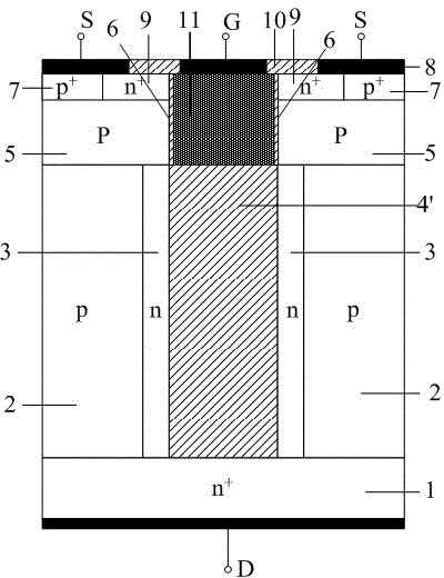
[0085] The manufacturing process of the semiconductor device of the present invention described in Embodiment 1 is preferably applied to a MOS control vertical device, so as to alleviate the contradictory relationship among withstand voltage, on-resistance and switching loss. used for Figure 6a with 6b It is a schematic diagram of the structure of an IGBT manufactured based on the manufacturing method of the present invention. Based on the manufacturing method of the present invention, the difference from Example 1 is that the initial semiconductor material substrate 1 is P + A semiconductor substrate 101, and a buffer layer 12 of the same conductivity type as that of the second semiconductor region is formed on the semiconductor substrate, and the buffer layer can improve the electrical characteristics of the IGBT. Epitaxially forming a first semiconductor region on the semiconductor buffer layer, and partially etching the first semiconductor region from the top to the sem...

Embodiment 3

[0087] The manufacturing process of the semiconductor device of the present invention described in Embodiment 1 can be applied to control vertical devices of N-channel MOS, and can also be applied to control vertical devices of P-channel MOS. P-channel DMOS as Figure 7a with 7b shown. When used in the manufacture of P-channel DMOS, the corresponding conductivity types of the semiconductor substrate 1, the semiconductor layer 2 of the first semiconductor region, the second semiconductor region 3, the active region 5, the body contact region 7, and the source region 9 are related to N The conductivity type of the corresponding region of the channel MOS control vertical device is opposite. Its key steps are as Figure 7c , Figure 7d with Figure 7e As shown, the subsequent steps are exactly the same as in Example 1. In Embodiment 1, an N-channel DMOS is manufactured, and the second semiconductor region 3 is formed by carving grooves on the epitaxial P-type semiconductor, ...


PUM


Abstract

The invention discloses a manufacturing method for a groove type semiconductor power device, relating to the technical field of the semiconductor power device. The manufacturing method comprises the following key technology steps of: growing and filling a groove by etching the groove and adopting an anisotropy epitaxy technology to form a second semiconductor region, locally etching at the top of the second semiconductor region to form a narrow high-concentration n or p column, filling an insulating medium and flattening, and afterwards, forming a body region by adopting laterally epitaxial overgrowth and the like. The manufacturing method has the advantages that the negative influences of the filling and planarization of the groove and the manufacturing and planarization of a groove gate on the formed body region, a body contact region and a source region are avoided; the bottom of the groove gate is flush with the lower interface of the body region or lower than the lower interface of the body region, thereby increasing the withstand voltage of the device; a complex mask is not needed, and the influence of a small-angle injection technology on a channel region is avoided; super junctions formed by adopting a multiple-time epitaxial injection manner and lattice defects caused by the super junctions are avoided; and the on-resistance is greatly reduced.

Description

[0001] technical field [0002] The invention relates to the technical field of semiconductor power devices, in particular to a method for manufacturing a low-power semiconductor power device with an extended dielectric groove and a groove gate structure. Background technique [0003] Power MOSFET is a multi-subconduction device, which has many advantages such as high input impedance, high frequency, and positive temperature coefficient of on-resistance. These advantages make it widely used in the field of power electronics, greatly improving the efficiency of electronic systems. [0004] The high voltage resistance of the device requires a long drift region and a low doping concentration in the drift region. However, as the length of the drift region increases and the doping concentration decreases, the on-resistance of the device ( ) increases, the on-state power consumption increases. Device on-resistance R on There is the following relationship with the breakdown ...

Claims


Application Information

Patent Timeline
Patent Type & Authority Applications(China)
IPC IPC(8): H01L21/336
Inventor 罗小蓉王沛蔡金勇范叶王琦蒋永恒周坤魏杰罗尹春范远航王骁伟
Owner UNIV OF ELECTRONICS SCI & TECH OF CHINA
Why Eureka
Try Eureka