Method and device for producing a semiconductor layer

A semiconductor and thin-layer technology, applied in semiconductor devices, semiconductor/solid-state device manufacturing, final product manufacturing, etc., can solve problems such as reducing the growth rate of the absorbing layer, improve electrical layer characteristics, reduce material costs, small purchase and maintenance The effect of fees

Inactive Publication Date: 2012-10-31
OC3 AG
View PDF5 Cites 17 Cited by
  • Summary
  • Abstract
  • Description
  • Claims
  • Application Information

AI Technical Summary

Problems solved by technology

This reduces the growth rate of the absorbing layer

Method used


Image

  • Method and device for producing a semiconductor layer
  • Method and device for producing a semiconductor layer

Examples


Embodiment Construction

[0036] In the following, the invention is elucidated by means of examples.

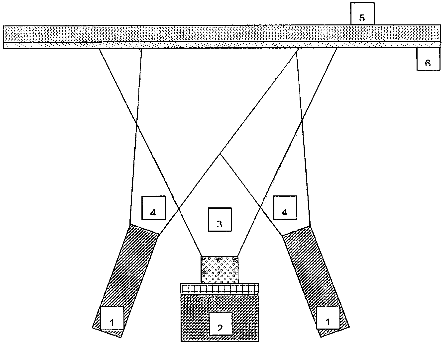
[0037] The substrate 5 provided with the molybdenum-countercontact layer 6 is placed in the coating chamber. In this case, the layer thickness of the molybdenum countercontact layer 6 lies in the range of 0.5 to 2 μm.

[0038] Now, in a vacuum process with 1×10 -6 and 1×10 -4 The pressure between mbar is coated with Cu(In,Ga)Se on the metal counter contact layer 6 2 semiconductor layer. Here, the metal components from the metal evaporator source 1 evaporate at a ratio of 0.81

[0039] The substrate holder is heated to a temperature between 400 and 550° C. during this coating step.

[0040] Through the setting of the metal evaporator 1 and the resulting ray guide area 4, and through the ion...


PUM

PropertyMeasurementUnit
thicknessaaaaaaaaaa
diameteraaaaaaaaaa

Abstract

The invention relates to a method and a device for producing a semiconductor layer. The problem addressed is that of increasing the deposition rate of the layer constituents and significantly improving the efficiency of a resulting solar cell. At the same time, the material costs are intended to be reduced. The problem is solved by virtue of the fact that, in a vacuum chamber, metal evaporator sources release Cu, In and / or Ga or the chalcogenide compounds, the latter are focused as metal vapour jets onto the substrate, and Se and / or S emerge(s) in an ionized fashion from a chalcogen low-energy wide-beam ion source and this beam is focused onto the surface of the substrate in such a way that it overlaps the metal vapour jets. A device for carrying out the method is described.

Description

technical field [0001] The invention relates to a method and a device for isolating copper-chlone absorber layers of thin-film solar cells on coating systems in a vacuum process, wherein a special low-energy broad-radiating particle source is used for the production. The development of highly efficient solar cells and their inexpensive fabrication are major goals in optoelectronics. In the development process, thin-film solar cells are of great significance and will open up a larger market share in the future, which is currently dominated by crystalline silicon solar cells. Background technique [0002] The corresponding absorber material employed in thin-film solar cells is CuInSe 2 and its alloy Cu(In,Ga)Se 2 Copper-chalcolide semiconductors Ⅰ-Ⅲ-Ⅵ 2 material system. A suitable thin-layer solar cell structure based on this absorber material consists of a glass substrate on which is coated a metallic counter-contact layer of molybdenum; this is then followed by a copper-...

Claims


Application Information

Patent Timeline
Patent Type & Authority Applications(China)
IPC IPC(8): H01L31/18C23C14/06C23C14/22H01L21/02C23C14/00H01L31/032
CPCH01L31/0322H01L31/0749C23C14/0031H01L21/02491H01L21/02568C23C14/0623H01L21/02631Y02E10/541Y02P70/50
Inventor 亨德里克·查赫曼卡斯滕·奥特霍斯特·诺依曼弗兰克·塑尔策卢茨·皮斯托尔
Owner OC3 AG
Why Eureka
Try Eureka