Method for improving conductive solder welding electronic packaging strength based on electrowetting principle
An electro-wetting, soldering technology, applied in welding equipment, circuits, electrical components, etc., can solve the problems of reduced welding strength and reliability of solder joints, and achieve the effect of low power consumption and remarkable effect.
- Summary
- Abstract
- Description
- Claims
- Application Information
AI Technical Summary
Problems solved by technology
Method used
Image

Examples
no. 1 example
[0050] In a first embodiment, the solder joint structure is single or multiple solder balls applied to a single substrate.
[0051] The method for improving the strength of an electronic package welded by conductive solder based on the electrowetting principle of the present invention includes: manufacturing a base substrate; and performing electrowetting treatment.
[0052] The making of described base substrate comprises:
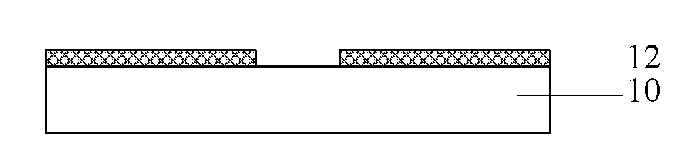
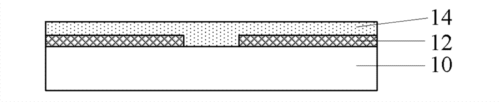
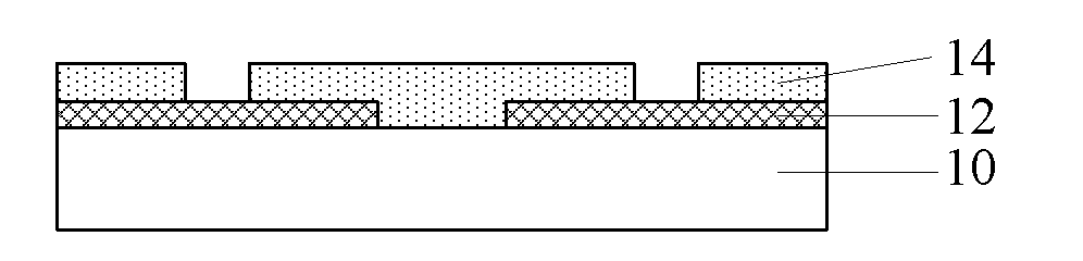
[0053] 1-1. Provide a substrate 10, form a metal layer 12 on the substrate 10, pattern the metal layer 12 to form a lower electrode, and form a Figure 1a structure shown.
[0054] In this embodiment, the method for forming the metal layer 12 is an evaporation process or a sputtering process, and the metal layer is to thickness of Ti / Au. The patterned metal layer 12 is used to form the lower electrode using a wet etching process (Wet Etching), which specifically includes: using photoresist as a mask, wet etching to form a pattern, and removing th...
no. 2 example
[0079] In the second embodiment, the solder joint structure is a single or multiple solder balls applied in a flip-chip soldering structure. As one of the most active chip bonding technologies currently researched and developed, flip-chip bonding technology can realize direct bonding between bumps and printed circuit boards or other substrates. It has small lead inductance, small crosstalk between signals, short signal transmission delay, and good electrical performance Good and other advantages, can achieve the highest installation density, the highest number of I / O and lower cost, etc., more suitable for high-frequency, high-speed electronic products, and have applications in communication fields such as mobile phones and optoelectronics.
[0080] It should be noted that, in the second embodiment, for the convenience of description, the substrate is a silicon wafer with good electrical conductivity as an example for illustration, and details can be found in the following desc...
no. 3 example
[0093] We know that in many MEMS and SIP structures, hermetic packages will be used. Therefore, in the third embodiment, the solder joint structure is a single or multiple solder rings applied to a hermetic package.
[0094] It should be noted that in the third embodiment, for the convenience of description, the substrate is a silicon wafer with good electrical conductivity as an example for illustration, and details are described in the following description.
[0095] The making of described base substrate comprises:
[0096] First, a first silicon substrate 30 is provided, and the first silicon substrate 30 is used as a first electrode; a second silicon substrate 31 is provided, and the second silicon substrate 31 is used as a second electrode;
[0097] Then, a first dielectric layer 32 is formed on the first silicon substrate 30; in this embodiment, the first dielectric layer 32 is silicon nitride or silicon oxide with a thickness of 1 μm to 5 μm.
[0098] A welding ring ...
PUM
| Property | Measurement | Unit |
|---|---|---|
| melting point | aaaaa | aaaaa |
| thickness | aaaaa | aaaaa |
| diameter | aaaaa | aaaaa |
Abstract
Description
Claims
Application Information
 - R&D
- Intellectual Property
- Life Sciences
- Materials
- Tech Scout
- Unparalleled Data Quality
- Higher Quality Content
- 60% Fewer Hallucinations
Browse by: Latest US Patents, China's latest patents, Technical Efficacy Thesaurus, Application Domain, Technology Topic, Popular Technical Reports.
© 2025 PatSnap. All rights reserved.Legal|Privacy policy|Modern Slavery Act Transparency Statement|Sitemap|About US| Contact US: help@patsnap.com