Manufacturing method for GaN-based film chip

A thin-film chip and temporary substrate technology, applied in electrical components, circuits, semiconductor devices, etc., can solve problems such as epitaxial film rupture, achieve the effects of reducing damage, improving yield, and reducing tear strength

Active Publication Date: 2012-11-21
晶能光電股份有限公司 +1
View PDF3 Cites 16 Cited by
  • Summary
  • Abstract
  • Description
  • Claims
  • Application Information

AI Technical Summary

Problems solved by technology

[0003] The technical problem to be solved by the present invention is to provide a method for preparing a GaN-based thin-film chi

Method used


Image

  • Manufacturing method for GaN-based film chip
  • Manufacturing method for GaN-based film chip
  • Manufacturing method for GaN-based film chip

Examples


specific Embodiment 1

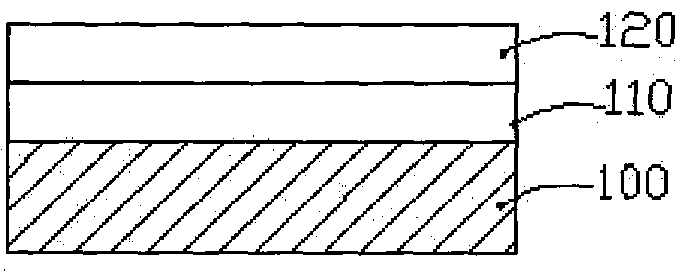
[0027] On the sapphire substrate, the n-type GaN layer, the active layer, and the p-type GaN layer were grown sequentially in MOCVD, and Ag was evaporated by electron beam evaporation as a reflective metal film, and then Cr / Pt / Au multilayer metal film was evaporated, at 500 ℃ alloy treatment. The sapphire substrate is thinned and polished so that the thickness of the sapphire substrate is 120 microns. Cut the sapphire substrate to obtain separated unit devices. Apply glue on the multi-layer metal film. The glue is a high-temperature epoxy resin modified glue. After curing, the Shore hardness is 80-100D, the temperature resistance range is -25-300°C, the tensile strength is 80-120MPa, compression Strength 200-300MPa. The thickness is 25 microns, bonded with the silicon substrate of the first temporary substrate, and cured at a temperature of 100° C. for 60 minutes. Laser peeling is carried out through the sapphire substrate surface, using a 248nm excimer laser with a power o...

specific Embodiment 2

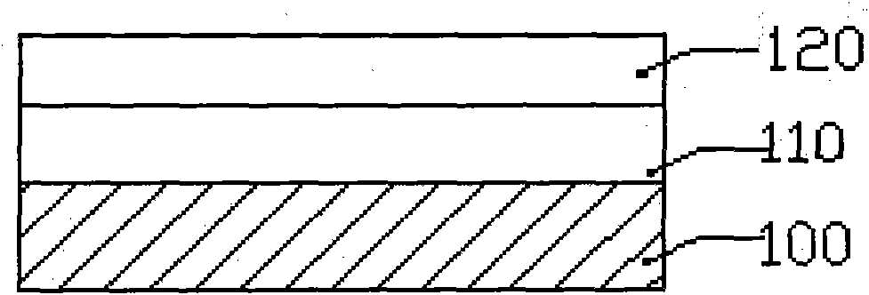
[0028] The n-type GaN layer, the light-emitting layer, and the p-type GaN layer are grown sequentially on the sapphire substrate, and Ag is deposited by electron beam evaporation as a reflective metal film and a multi-layer metal film Cr / Pt / Au, and alloyed at 500 °C. The sapphire substrate was thinned and polished so that the thickness of the sapphire was 150 microns. The sapphire substrate is cut, and the sapphire unit is glued. The glue is a high-temperature epoxy resin modified glue with a thickness of 20 microns. It is bonded with the silicon substrate and cured at 120°C for 40 minutes. Laser lift-off is performed through the sapphire surface, using a 193nm excimer laser with a power of 480 mW. The peeled sapphire unit is then coated with another glue—modified heterocyclic resin, and cured at 120°C for 60 minutes. First corrode the silicon substrate with hydrofluoric acid plus hydrogen peroxide plus nitric acid (5:2:2), then use acetamide to corrode the high-temperature ep...

specific Embodiment 3

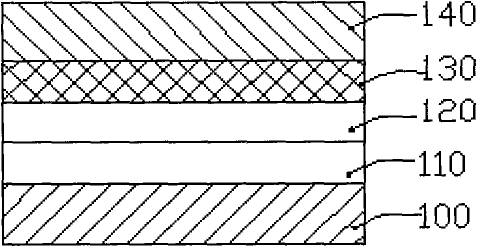
[0029] The buffer layer, n-type GaN layer, light-emitting layer, p-type GaN, etc. are sequentially grown on the sapphire substrate by MOCVD, and AgPt is evaporated as a reflective composite layer, and alloyed at 500 ° C. The obtained epitaxial wafer was waxed and polished so that the thickness of the sapphire was 400 micrometers. The sapphire substrate is cut, and the sapphire unit is glued. The glue is a high-temperature epoxy resin modified glue with a thickness of 60 microns. It is bonded with the sapphire substrate and cured at 120°C for 60 minutes. Laser lift-off is performed through the sapphire surface, using a 248nm excimer laser with a power of 550 mW. The peeled sapphire unit is then coated with another modified heterocyclic resin, bonded to the silicon substrate, and cured at 120°C 60 minutes. Use acetamide to corrode the high-temperature epoxy resin modified adhesive at 120°C to remove the sapphire substrate, and protect the second adhesive with wax. Then Au-Sn i...


PUM

PropertyMeasurementUnit
Temperature resistantaaaaaaaaaa
Compressive strengthaaaaaaaaaa
Thicknessaaaaaaaaaa

Abstract

The invention provides a manufacturing method for a GaN-based film chip and relates to a manufacturing process of semiconductor light-emitting devices. According to the manufacturing method, the problem that an epitaxial film is broken when a sapphire substrate is stripped is solved. The manufacturing method comprises the following steps: sequentially growing an n-type GaN layer, an active layer and a p-type GaN layer on the sapphire substrate to form a semiconductor multilayer structure; carrying out thinning and polishing treatment on the sapphire substrate; coating a first adhesive on the semiconductor multilayer structure and a conducting reflective composite metal layer and curing the first adhesive with a first temporary substrate; carrying out laser stripping on the sapphire substrate, coating a second adhesive on the stripping surface and curing the second adhesive to a second temporary substrate; removing the first temporary substrate and the first adhesive; combining the semiconductor multilayer structure with a permanent support substrate by adopting an eutectic bonding way; and removing the second temporary substrate and the second adhesive. According to the manufacturing method disclosed by the invention, the damage to a GaN film can be reduced and the yield of a GaN-based film chip obtained by the process can be greatly increased.

Description

technical field [0001] The invention relates to a preparation process of a semiconductor light emitting device. More specifically, the present invention relates to a method for preparing a GaN-based thin film chip by using a laser lift-off process. Background technique [0002] The sapphire substrate is the main substrate for GaN-based LED epitaxial growth, and its conductivity and heat dissipation are relatively poor. Due to poor conductivity, light-emitting devices have to adopt a lateral structure, resulting in current blockage and heat generation. And poor thermal conductivity limits the power of light emitting devices. After the sapphire substrate is removed by laser lift-off technology, the light-emitting diode is made into a vertical structure, which can effectively solve the problem of heat dissipation and light output. The low yield rate is the bottleneck of the industrialization of laser lift-off sapphire substrate technology. Due to the stress generated by the...

Claims


Application Information

Patent Timeline
IPC IPC(8): H01L33/00
Inventor 闫占彪赵汉民朱浩周印华熊传兵陈栋
Owner 晶能光電股份有限公司
Why Eureka
Try Eureka