
Micro atomic cavity subjected to negative pressure forming, micro atomic clock chip and preparation method for micro atomic cavity and micro atomic clock chip

A technology of atomic cavity and atomic clock, which is applied in the field of MEMS (micro-electro-mechanical system) manufacturing, can solve the problems of high design requirements, high cost, and complicated assembly of reflective surfaces, and achieve low cost, simple method, and low cost.

Inactive Publication Date: 2012-12-05
SOUTHEAST UNIV
View PDF5 Cites 12 Cited by
  • Summary
  • Abstract
  • Description
  • Claims
  • Application Information

AI Technical Summary

Problems solved by technology

The problem with this design method is that the assembly is more complicated, and the design requirements for the reflective surface are higher, so the cost is higher

Method used


Image

  • Micro atomic cavity subjected to negative pressure forming, micro atomic clock chip and preparation method for micro atomic cavity and micro atomic clock chip
  • Micro atomic cavity subjected to negative pressure forming, micro atomic clock chip and preparation method for micro atomic cavity and micro atomic clock chip
  • Micro atomic cavity subjected to negative pressure forming, micro atomic clock chip and preparation method for micro atomic cavity and micro atomic clock chip

Examples


Embodiment 1

[0041] A preparation method for negative pressure forming miniature atomic cavities, comprising the following steps:

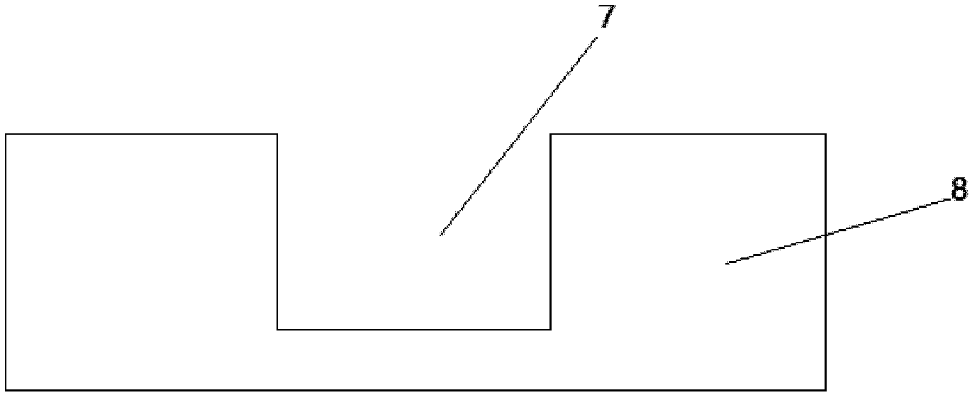
[0042] The first step is to use deep reactive ion etching technology to etch a square deep groove on the silicon wafer to form a silicon mold;

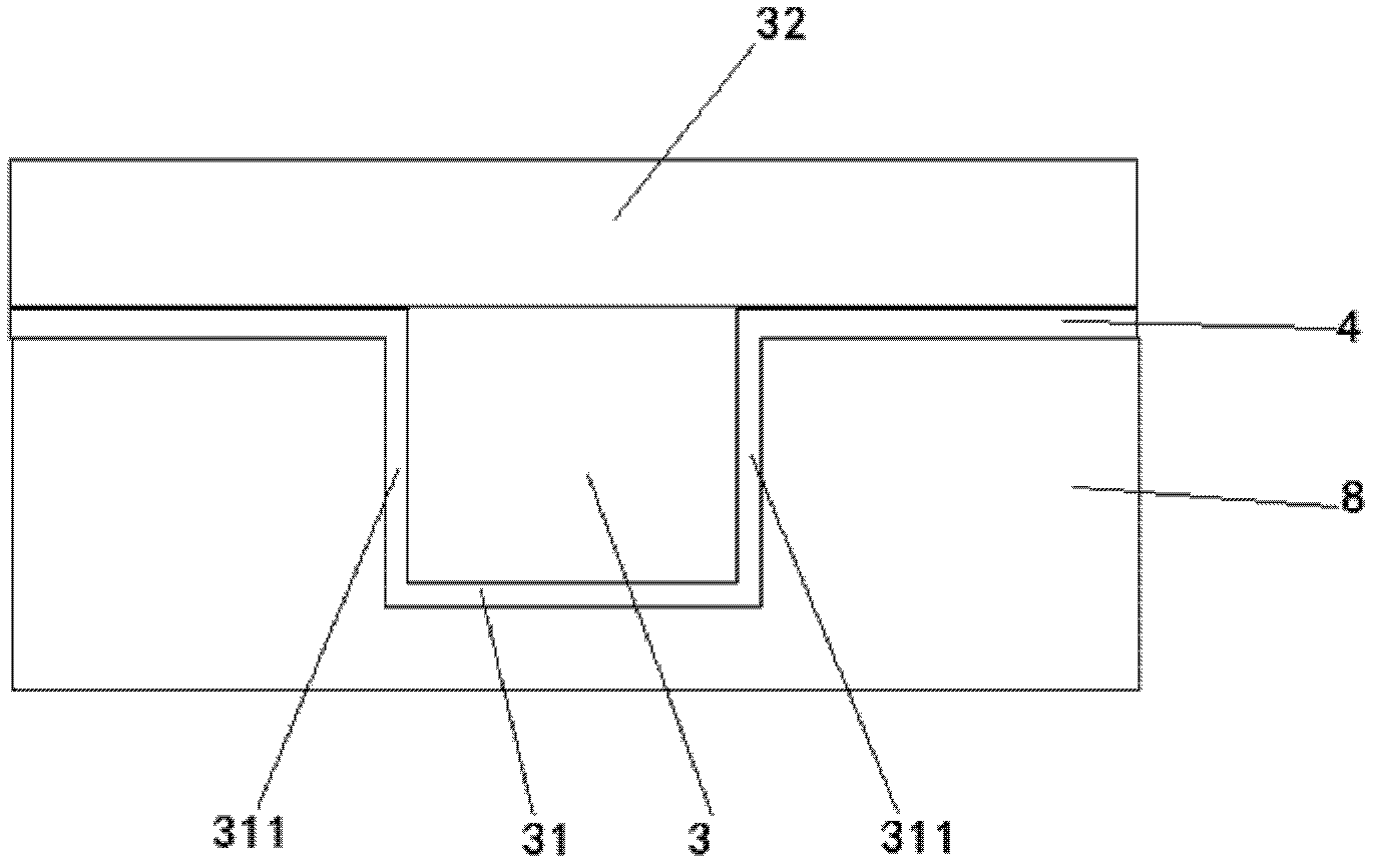
[0043] In the second step, anodically bond the above-mentioned silicon mold with deep grooves and the Pyrex borosilicate glass assembly wafer under vacuum. The anodic bonding conditions are: the temperature is 300-500°C, for example, 300°C, 400°C and 500°C, the voltage is 400-800V, for example, 400V, 600V, and 800V can be selected, so that the borosilicate glass wafer and the above-mentioned deep groove form a sealed cavity;

[0044] The third step is to heat the bonded wafer above the glass softening temperature under an atmospheric pressure, for example, 1270°C, and keep it warm at this temperature for 10-30 minutes, for example, 10min, 20min, 30min , the pressure difference inside and outside the cavity makes the ...

Embodiment 2

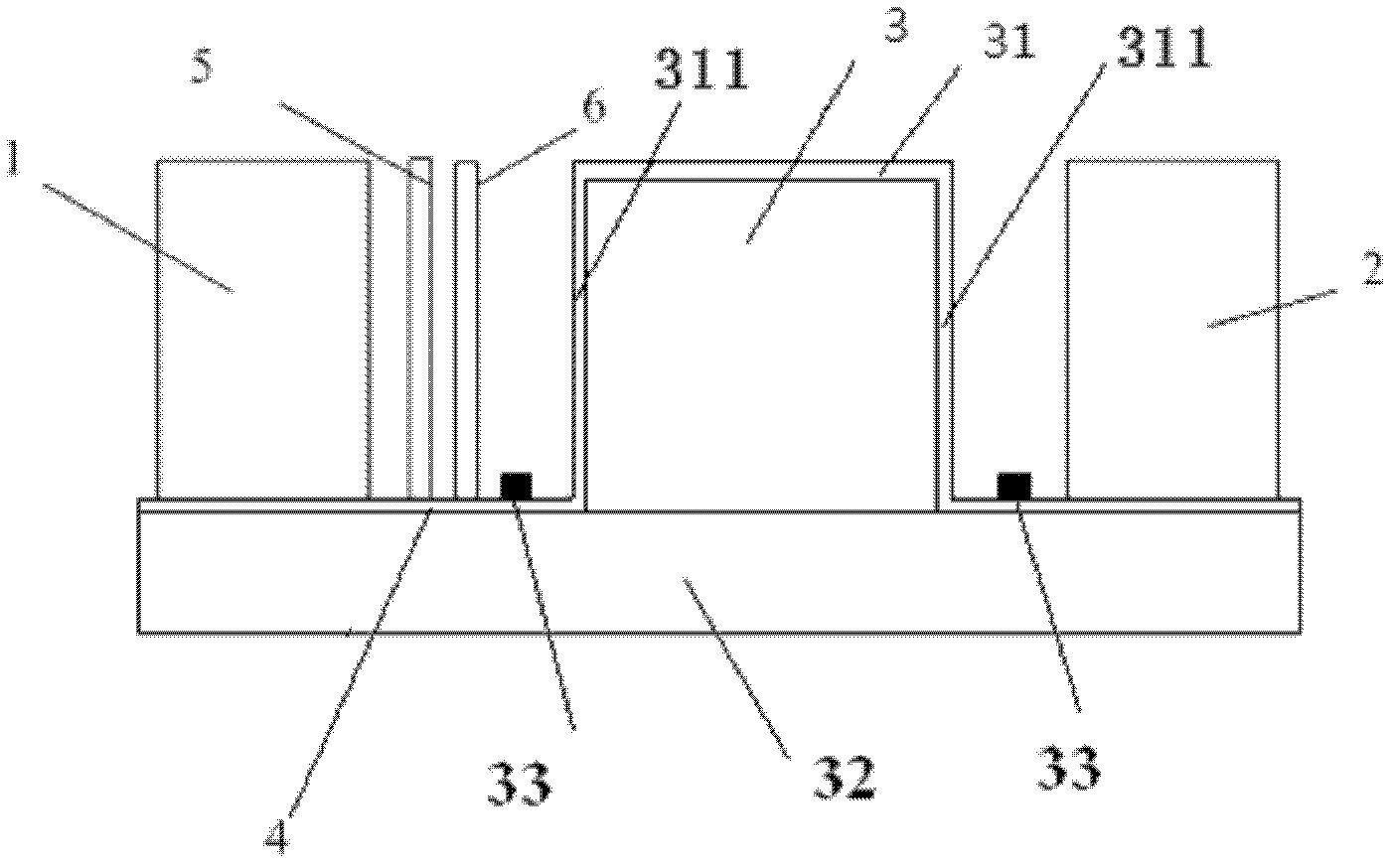
[0048] A miniature atomic clock chip comprises a laser generator, a filter, a quarter wave plate, a laser detector and the miniature atomic cavity prepared by the method, a laser generator, a filter, a quarter wave plate, a laser detector They are all assembled on borosilicate glass assembly wafers, and their centers are on the same optical axis as the center of the glass microcavity. The laser generator is located on the side of the airtight glass atomic cavity with a straight vertical side. A filter and a quarter-wave plate are arranged in sequence between the straight and vertical sides. The laser light emitted by the laser generator passes through the filter and the quarter-wave plate, enters the airtight glass atomic cavity through the straight and vertical sides, and then passes through the glass The other straight and vertical side of the microcavity exits and is detected by a laser detector. A heater is also arranged around the glass microcavity. The above-mentioned hea...

Embodiment 3

[0050] A preparation method for a miniature atomic clock chip, comprising the following steps:

[0051] In the first step, a micro-atomic cavity with straight and vertical sides is prepared by negative pressure forming method;

[0052] In the second step, a heater is prepared on the borosilicate glass assembled wafer around the glass microcavity;

[0053] In the third step, the laser generator, laser detector, filter and quarter-wave plate are respectively assembled on the corresponding positions of the borosilicate glass assembly wafer and are located at the same position as the center of the straight vertical side of the airtight glass atomic cavity. On one optical axis, the laser light emitted by the laser generator can be detected by the laser detector after passing through the filter, the quarter-wave plate and the sealed glass atomic cavity;

[0054] The fourth step is to prepare the pins of the heater, laser generator and laser detector, and connect them to the power s...


PUM


Abstract

The invention discloses a micro atomic cavity subjected to negative pressure forming, a micro atomic clock chip and a preparation method for the micro atomic cavity and the micro atomic clock chip. The method comprises the following steps of: etching a deep groove to form a silicon die; performing anodic bonding on the silicon die and a borosilicate glass assembled wafer under vacuum to form a sealed cavity; heating the wafer to temperature higher than glass transition temperature, preserving heat, cooling, and performing stress relief annealing on the wafer; putting a substance necessary to an atomic clock into the formed glass micro cavity, pre-bonding the glass micro cavity and a silicon substrate at room temperature in nitrogen atmosphere to seal the glass micro cavity, keeping pressure, and performing anodic bonding to obtain a sealed glass atomic cavity; corroding, and removing the silicon die to obtain a micro atomic cavity with straight vertical sides; preparing heaters on the borosilicate glass assembled wafer at the periphery of the glass micro cavity, and assembling components at the corresponding positions of the borosilicate glass assembled wafer; and preparing pins, and connecting the pins, a power supply and a processing circuit. The method is simple and low in cost.

Description

technical field [0001] The invention designs a MEMS (micro-electro-mechanical system) manufacturing technology, and in particular relates to a negative-pressure forming miniature atomic cavity, a miniature atomic clock chip and a preparation method. [0002] Background technique [0003] At present, atomic clocks are the most accurate artificial clocks, and the accuracy of atomic clocks can reach one billionth of a second or even higher. A special type of quantum transition in atomic clocks is the hyperfine transition, which involves the interaction of the nuclear magnetic field of the atom and the magnetic field of the electrons outside the nucleus. In principle, the principle of atomic clocks is basically clear, and there are two main directions for current development: one is to improve the performance of atomic clocks in terms of accuracy; the other is to miniaturize them while ensuring their performance. Currently, the world's most accurate atomic clock is in Colorado...

Claims


Application Information

Patent Timeline
Patent Type & Authority Applications(China)
IPC IPC(8): B81B7/00B81C1/00G04F5/14
Inventor 尚金堂王亭亭魏文龙蒯文林秦顺金于慧
Owner SOUTHEAST UNIV
Learn More