Method for preparing aluminum nitride single crystal material
A single crystal material, aluminum nitride technology, applied in polycrystalline material growth, chemical instruments and methods, single crystal growth, etc., can solve problems such as bending and cracking of high-density dislocation films that are difficult to overcome, and achieve good practicality Effects on Value and Marketing Prospects
- Summary
- Abstract
- Description
- Claims
- Application Information
AI Technical Summary
Problems solved by technology
Method used
Image

Examples
preparation example Construction
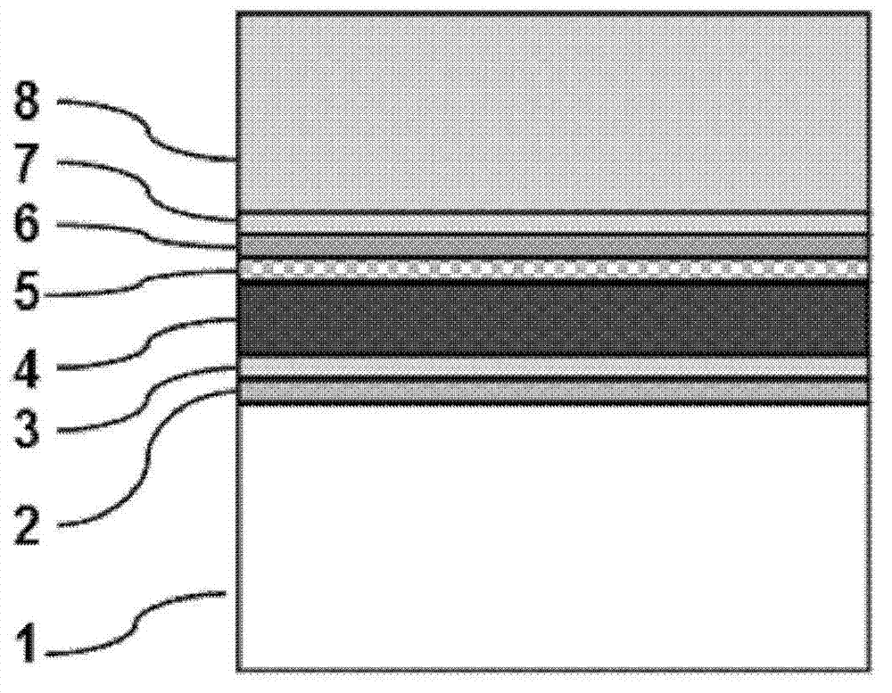
[0025] see figure 1 As shown, the present invention provides a method for preparing an aluminum nitride single crystal material, which is characterized in that it comprises the following steps:
[0026] Step 1: Put a substrate 1 into the growth chamber of metal organic chemical vapor deposition-halide vapor phase epitaxy compound process equipment, the substrate 1 is a high melting point heterogeneous single crystal substrate, its melting point is higher than 1300°C and Sapphire, silicon carbide or gallium nitride materials that have a good lattice matching relationship with aluminum nitride;
[0027] Step 2: Prepare a III-nitride nucleation layer 2 on the substrate 1 by metal-organic chemical vapor deposition process, the III-nitride nucleation layer 2 is GaN, AlN or AlGaN material, and the preparation temperature is 300 to 700°C, with a thickness of 5 to 500nm;
[0028] Step 3: heating the substrate 1 to a higher temperature, and preparing a III-nitride crystalline layer 3...
Embodiment 1
[0046] The process of preparing aluminum nitride (AlN) thick film single crystal material and aluminum nitride (AlN) bulk single crystal material by using sapphire (a-Al2O3) material as heterogeneous single crystal substrate is as follows:
[0047] Step 1: Place a 2 inch diameter a-Al 2 o 3 The single crystal substrate material 1 is placed in the growth chamber of the MOCVD-HVPE compound process equipment;
[0048] Step 2: Prepare a 30nm-thick GaN low-temperature nucleation layer 2 on the sapphire single crystal substrate material at a low temperature at a substrate heating temperature of 550° C. by using a gold MOCVD process;
[0049] Step 3: raising the substrate heating temperature to 1050° C., and preparing a 500 nm thick GaN high-temperature crystallization layer 3 on the GaN low-temperature nucleation layer 2 at high temperature by using the MOCVD process;
[0050] Step 4: Lower the heating temperature of the substrate to 600°C, and prepare a 50nm-thick TiN stress-conf...
Embodiment 2
[0061] The process flow of using silicon carbide (6H-SiC) material as heterogeneous single crystal substrate to prepare aluminum nitride (AlN) thick film single crystal material and AlN bulk single crystal material is as follows:
[0062] Step 1: Put the 6H-SiC single crystal substrate material 1 with a diameter of 2 inches and a thickness of 300 microns into the growth chamber of the MOCVD-HVPE composite process equipment;
[0063] Step 2: Prepare a 20nm-thick AlN low-temperature nucleation layer 2 on a 6H-SiC single crystal substrate material at a low temperature with a substrate heating temperature of 650° C. by MOCVD process;
[0064] Step 3: raising the heating temperature of the substrate to 1300°C, and preparing a 300nm thick AlN high-temperature crystallization layer 3 on the AlN low-temperature nucleation layer 2 at high temperature by MOCVD process;
[0065] Step 4: Lower the heating temperature of the substrate to 650°C, and prepare a 50nm-thick HfN stress-consisten...
PUM
| Property | Measurement | Unit |
|---|---|---|
| Melting point | aaaaa | aaaaa |
| Thickness | aaaaa | aaaaa |
| Thickness | aaaaa | aaaaa |
Abstract
Description
Claims
Application Information
 - R&D
- Intellectual Property
- Life Sciences
- Materials
- Tech Scout
- Unparalleled Data Quality
- Higher Quality Content
- 60% Fewer Hallucinations
Browse by: Latest US Patents, China's latest patents, Technical Efficacy Thesaurus, Application Domain, Technology Topic, Popular Technical Reports.
© 2025 PatSnap. All rights reserved.Legal|Privacy policy|Modern Slavery Act Transparency Statement|Sitemap|About US| Contact US: help@patsnap.com