Thin film transistor and manufacturing method thereof
一种薄膜晶体管、制造方法的技术,应用在晶体管、半导体/固态器件制造、半导体器件等方向,能够解决影响薄膜晶体管电性、氧化物半导体层损伤、降低薄膜晶体管质量等问题,达到缩短生产时间、降低生产成本、提高质量的效果
- Summary
- Abstract
- Description
- Claims
- Application Information
AI Technical Summary
Problems solved by technology
Method used
Image

Examples
Embodiment Construction
[0049] In order to further illustrate the technical means adopted by the present invention and its effects, the following describes in detail in conjunction with preferred embodiments of the present invention and accompanying drawings.
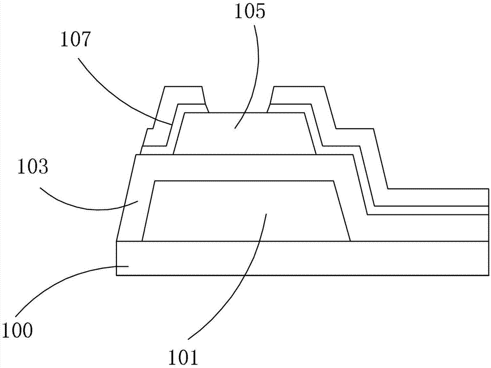
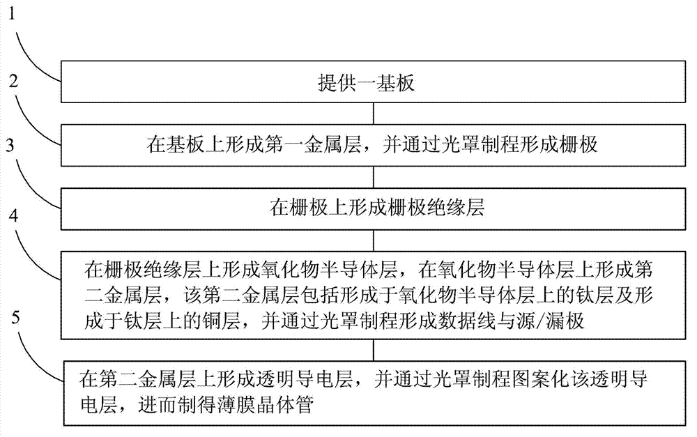
[0050] see Figure 2 to Figure 11 , the invention provides a method for manufacturing a thin film transistor, comprising the following steps:
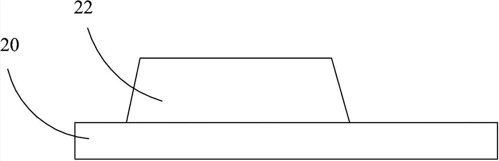
[0051] Step 1, providing a substrate 20 .
[0052]The substrate 20 is a transparent substrate, preferably a glass or plastic substrate.
[0053] Step 2, forming a first metal layer 22 on the substrate 20, and forming a gate through a photomask process.
[0054] The first metal layer 22 is copper (Cu), aluminum (Al), molybdenum (Mo), titanium (Ti) or a stacked structure thereof.
[0055] Step 3, forming a gate insulating layer 24 on the gate.
[0056] The gate insulating layer 24 is silicon oxide (SiO x ) or silicon nitride (SiN x ) layer formed on the first metal layer 22 by chemical vapor deposi...
PUM
 Abstract
Description
Claims
Application Information
 - R&D
- Intellectual Property
- Life Sciences
- Materials
- Tech Scout
- Unparalleled Data Quality
- Higher Quality Content
- 60% Fewer Hallucinations
Browse by: Latest US Patents, China's latest patents, Technical Efficacy Thesaurus, Application Domain, Technology Topic, Popular Technical Reports.
© 2025 PatSnap. All rights reserved.Legal|Privacy policy|Modern Slavery Act Transparency Statement|Sitemap|About US| Contact US: help@patsnap.com