

Etching process for semiconductors
A semiconductor and etching technology, applied in semiconductor devices, semiconductor/solid-state device manufacturing, electrical components, etc., can solve problems such as rough surfaces and low etching rates
- Summary
- Abstract
- Description
- Claims
- Application Information
AI Technical Summary
Problems solved by technology
Method used
Image

Examples
example
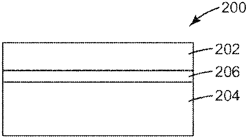
[0034] A II-VI semiconductor color conversion layer structure based on a CdMgZnSe alloy was grown by molecular beam epitaxy on an InP substrate. The color conversion layer structure is schematically shown in figure 2 , and the layer thicknesses and compositions are shown in Table I below. figure 2 It is a schematic diagram of the color conversion layer 200 , which includes a top window 202 , a light absorbing layer 204 , and a graded composition layer 206 whose composition gradually changes from the composition of the top window 202 to the composition of the light absorbing layer 204 . Embedded in the light-absorbing layer (not shown) are quantum wells that trap carriers produced when pump light is absorbed in the light-absorbing layer and re-emit longer wavelength light. Details of color converting structures can be found, for example, in US Patent No. 7,402,831 (Miller et al.).
[0035] Table I
[0036] Composition of the color conversion layer structure
[0037] ...
example 1
[0041] Example 1 - Ar etching of II-VI semiconductor with photoresist mask
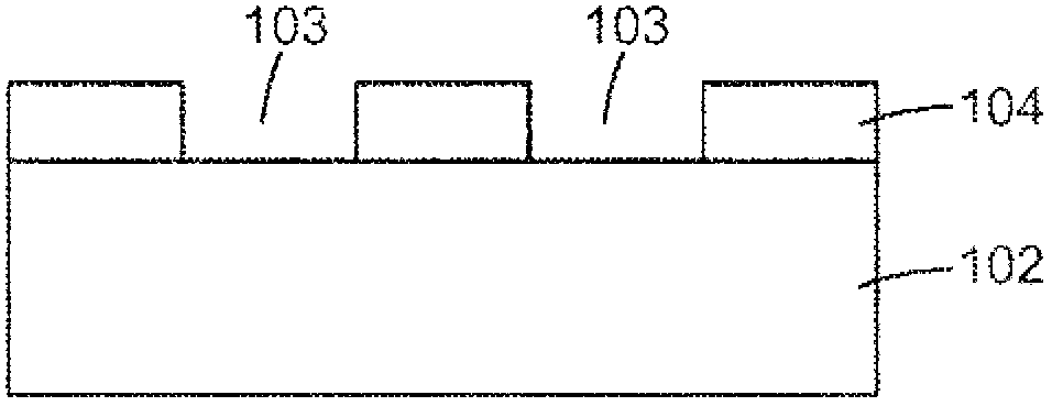
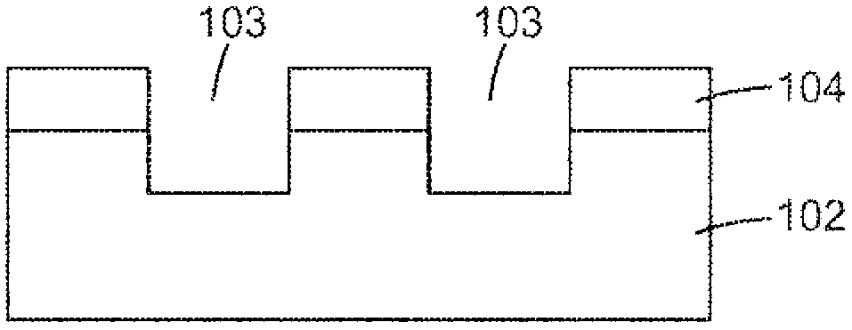
[0042] A sample of the II-VI semiconductor color converter described above was coated with a photoresist mask with a stripe pattern using NR9-1000P negative photoresist (from Futerrex, Franklin, NJ). The dimensions of the stripe patterns are 2 μm and 100 μm. Small split samples of II-VI semiconductors with photoresist masks on them were placed on Si carrier wafers, loaded into the RIE chamber, and heated using 5-50 sccm Ar, 20-200 watts Rf power, 700-2000 Watts Inductively Coupled Plasma Power (ICP) Plasma etching was performed at a pressure of 4-30 mTorr and an etching time of 5 x 60 second intervals. Pixel stripes as small as 2 μm in width continued to exhibit strong photoluminescence several months after treatment. With the same conditions as in Comparative Example 1, with the 2 The same sample etched showed rapid degradation of photoluminescence after one day. image 3 A photomicrograph of a...
example 2
[0043] The Ar etching of 3 micron channel in the example 2-II-VI group semiconductor material
[0044]The patterned photoresist on the II-VI semiconductor color converter structure as described above in Table 1 was obtained by photolithography with NR9-3000PY negative photoresist (available from Futurrex, Franklin, NJ) and etched using the procedure of Example 1. Figure 4a is a scanning electron micrograph of the resulting structure and shows a pattern of 3 μm wide channels with ~6 μm bumps in between. Figure 4b Darkfield optical micrograph showing photoluminescence of semiconductor bumps. A series of emission "pixels" were observed in which the semiconductor color converter had been left untouched (protected by photoresist during etching).
PUM
 Abstract
Description
Claims
Application Information