Simple preparation method and application of polydimethylsiloxane (PDMS) polymer microlens array

A micro-lens array and polymer technology, which is applied to lenses, micro-lithography exposure equipment, and photo-engraving processes of patterned surfaces, can solve the problems of high price and complicated operation, and achieve the effect of simple operation and low experimental cost.

Active Publication Date: 2013-03-13
DALIAN INST OF CHEM PHYSICS CHINESE ACAD OF SCI
View PDF7 Cites 20 Cited by
  • Summary
  • Abstract
  • Description
  • Claims
  • Application Information

AI Technical Summary

Problems solved by technology

[0004] The purpose of the present invention is to provide a simple preparation method and application of PDMS polymer microlens array, which solves the problems of complex operation and high price in the previous production process.

Method used


Image

  • Simple preparation method and application of polydimethylsiloxane (PDMS) polymer microlens array
  • Simple preparation method and application of polydimethylsiloxane (PDMS) polymer microlens array
  • Simple preparation method and application of polydimethylsiloxane (PDMS) polymer microlens array

Examples


Embodiment 1

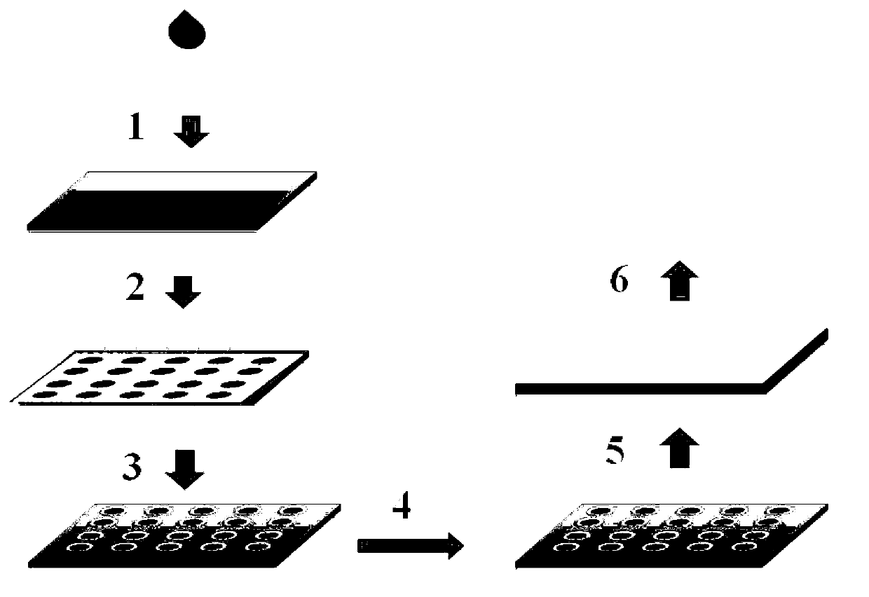
[0036] The preparation of embodiment 1PDMS polymer lens array

[0037] The SU-8 polymer template was fabricated by photolithography technology, and the template contained a circular hole with a diameter of 50 microns. The whole PDMS polymer lens array preparation process is as follows: figure 1 As shown, apply SU-8 photoresist on a clean glass sheet, adjust the thickness of the glue (100 microns to 1 mm) according to needs, heat at 95 degrees Celsius for 1 hour to evaporate the solvent in the photoresist; put the designed mask The film was exposed to ultraviolet light for 60 seconds; placed in the developer solution ethyl lactate for development, the development time was adjusted according to needs (1~15 minutes), and then heated at 80°C for 5 minutes to make the remaining unexposed SU8 photoresist Thermal fusion occurs, and the schematic diagram before and after thermal fusion is as follows figure 2 Shown; finally exposed under the UV lithography machine for 120 seconds to...

Embodiment 2

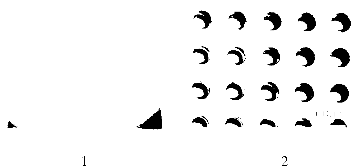
[0038] Embodiment 2 Preparation of different height PDMS polymer lens arrays

[0039] By controlling the development time to 1 minute, 2 minutes, 3 minutes, 4 minutes, 5 minutes, and 10 minutes, gradually increase the amount of unexposed SU8 photoresist removed to realize the control of the microwell depth in the SU8 template. PDMS polymer lens arrays prepared using templates with different conditions such as Figure 5-10 shown.

Embodiment 3

[0040] Embodiment 3 Imaging Research of PDMS Polymer Lens Array

[0041] This process is realized by an optical microscope. An object image is placed under the prepared PDMS polymer microlens array. By adjusting the height of the lens and the object image to find a suitable focal length, each lens on the microlens array can be observed in a certain area. All can display the image of the object, and the object image of this experiment adopts the printed letter A. At the same time, lenses of different sizes are used to achieve imaging of different sizes (imaging effects such as Figure 11-14 shown).


PUM


Abstract

The invention discloses a simple preparation method and an application of a polydimethylsiloxane (PDMS) polymer microlens array. The preparation method comprises the following steps of: exposing a graph designed by a lithography method on an SU8 photoresist, developing the graph by employing a developing solution, and controlling the developing time, so that the unexposed SU8 photoresist part is removed; baking the unexposed SU8 photoresist part in an oven, so that the bottom is in an arc shape; taking the unexposed SU8 photoresist part out, cooling to room temperature, and performing secondary exposure, so that the SU8 is completely cured and is manufactured into a template for manufacturing a PDMS polymer lens; and pouring the non-cured PDMS polymer solution to the template, heating and curing the PDMS polymer solution, and stripping a PDMS chip to manufacture the PDMS polymer microlens array. The prepared PDMS can be applied to optical imaging; and the method is simply and rapidly operated, is low in experimental cost and can be integrated with other technologies.

Description

technical field [0001] The invention belongs to the field of optical lens preparation, and in particular provides a simple preparation method and application of a PDMS polymer microlens array. Background technique [0002] Microlens array is an important type of optical element in array optical devices. It is an array composed of a series of tiny lenses with apertures ranging from a few microns to hundreds of microns. The microlens array has small size, light weight, It has the advantages of easy integration and other advantages, and plays an important role in various fields such as military affairs and scientific research. The production methods of microlens array mainly include: grayscale mask technology, laser direct writing technology, ion exchange method, photosensitive glass thermoforming method, photoresist hot melting method, sol-gel method, micro-jet printing method, hard mold or Soft mold imprinting technology, photoelectric reactive etching, focused ion beam etch...

Claims


Application Information

Patent Timeline
Patent Type & Authority Applications(China)
IPC IPC(8): G02B3/00G03F7/00G03F7/20
Inventor 秦建华姜雷朱国丽
Owner DALIAN INST OF CHEM PHYSICS CHINESE ACAD OF SCI
Why Eureka
Try Eureka