Electron beam overlay marking based on hafnium dioxide and its manufacturing method

A technology of hafnium dioxide and its production method, which is applied to the photoplate making process of the patterned surface, circuits, electrical components, etc., and can solve the problems of poor adhesion between gold and silicon substrates, expensive gold targets, and metal melting deformation. , to achieve strong adhesion, lower production costs, and high alignment accuracy

Inactive Publication Date: 2015-08-26
HUAZHONG UNIV OF SCI & TECH
View PDF11 Cites 0 Cited by
  • Summary
  • Abstract
  • Description
  • Claims
  • Application Information

AI Technical Summary

Problems solved by technology

However, the "titanium + gold" mark also has its disadvantages: the price of gold target is very expensive; the adhesion between gold and silicon substrate is very poor, and titanium plating is needed to adhere gold and silicon together; the melting point of gold is 1063 ° C, If the sample needs to be used in high-temperature thermal oxidation or epitaxial growth processes, metal melting deformation and metal diffusion will occur, and then the cavity of oxidation or epitaxial growth will be polluted, which will bring very serious consequences.

Method used


Image

  • Electron beam overlay marking based on hafnium dioxide and its manufacturing method
  • Electron beam overlay marking based on hafnium dioxide and its manufacturing method
  • Electron beam overlay marking based on hafnium dioxide and its manufacturing method

Examples


Embodiment

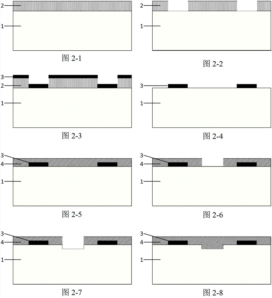
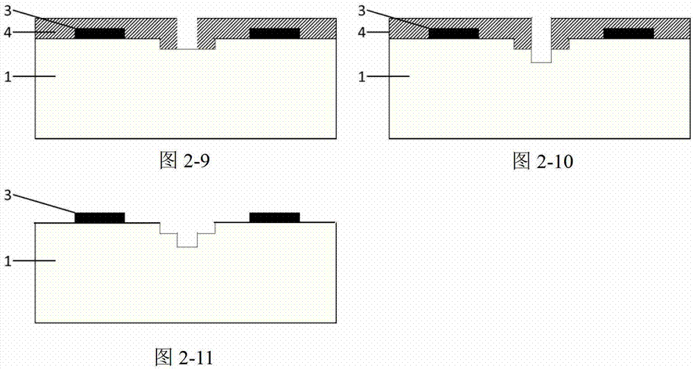
[0054] Example: Experimental measurement of hafnium dioxide overlay accuracy.

[0055] Design layout such as image 3 , the left and right parts respectively represent the A and B two-layer waveguides that need to be engraved. The width of the waveguide (that is, the blank part between the white strips and the shadow strips) is 500nm, and the vertical arrangement interval of the waveguides in the B layer is 2.5μm; the position deviation of the waveguide in the center of the A and B layers in the y direction is 0 , along the y-axis positive and negative A-layer waveguide arrangement period is 25nm larger than B-layer waveguide arrangement period. Use positive electronic resist ZEP520 as a mask, and use ICP to etch about 200nm on the substrate after electron beam overlay exposure; after the two-layer waveguide etching is completed, send the sample to the scanning electron microscope to measure the alignment error (such as Pic 4-1 ,4-2). Pic 4-1 , 4-2 represent the overlay a...


PUM

PropertyMeasurementUnit
thicknessaaaaaaaaaa
thicknessaaaaaaaaaa

Abstract

The invention discloses an electron beam aligning mark based on hafnium oxide, which belongs to the field of micro and nano fabrication of a semi-conductor device. The electron beam aligning mark based on hafnium oxide comprises a substrate and a hafnium oxide thin film mark plated on the substrate. The invention further provides a manufacturing method which specifically comprises the steps of: (1) cleaning the substrate; (2) carrying out spin coating of an electronic resist on the substrate and forming a pattern array with an aligned mark in the electronic resist through an electron beam photolithography technique; (3) evaporating hafnium oxide thin films on the electronic resist and the substrate; and (4) peeling the hafnium oxide thin films attached to the positive electronic resist to obtain the hafnium oxide mark. The aligned mark obtained by the electron beam lithography is prepared by using hafnium oxide which is high temperature resistive, good in adhesion and low in cost. Compared with the conventional 'titanium+gold' marks, the process cost is reduced, the problem that the gold mark and the Si substrate are not adhered well is solved, the adhesion and high temperature bearing capacity of the aligned mark to the substrate are improved, and the higher aligning precision is maintained.

Description

technical field [0001] The invention belongs to the field of micro-nano manufacturing of semiconductor devices, and in particular relates to an electron beam lithography overlay mark based on hafnium dioxide and a manufacturing method thereof. Background technique [0002] The semiconductor technology with Complementary Metal Oxide Semiconductor (CMOS, Complementary Metal Oxide Semiconductor) process as the mainstream continues to develop rapidly along "Moore's Law". More and more stringent requirements are put forward for the accuracy of the semiconductor process. Only by minimizing the accuracy error of each link in the process can the device failure caused by the error be reduced. [0003] The electron beam lithography system plays an increasingly important role in the micro-nano manufacturing process of semiconductor devices due to its advantages of high precision and no need for masks. In the micro-nano manufacturing of semiconductor devices, the manufacture of a devic...

Claims


Application Information

Patent Timeline
Patent Type & Authority Patents(China)
IPC IPC(8): H01L23/544H01L21/02G03F9/00
Inventor 曾成夏金松张永
Owner HUAZHONG UNIV OF SCI & TECH
Why Eureka
Try Eureka