LED (light emitting diode) packaged based on zinc oxide-bismuth oxide composite ceramic substrate and preparation method thereof

A technology of composite ceramics and base piezoceramics, applied in electrical components, electrical solid devices, circuits, etc., can solve the problems of easy breakdown of PN junctions, and achieve simple electrical circuits, strong resistance to instantaneous current inrush, and high efficiency. Effect

Active Publication Date: 2013-04-17
泰州市华强照明器材有限公司
View PDF4 Cites 15 Cited by
  • Summary
  • Abstract
  • Description
  • Claims
  • Application Information

AI Technical Summary

Problems solved by technology

ZnO is an N-type semiconductor material, while Bi 2 o 3 It is a weak P-type semiconductor material, so that countless PN and NP phases are connected in series at the boundaries of multiple ZnO particles. The network, as shown in the schematic diagram figure 2 As shown, this can greatly improve the resistivity of the material, and at low voltage, half of the PN and NP junctions are reversed, and the total resistance of the material is very large, but at high voltage, half of the PN junctions are easily reversed. Breakdown, similar to a Zener diode, instantaneous conduction

Method used


Image

  • LED (light emitting diode) packaged based on zinc oxide-bismuth oxide composite ceramic substrate and preparation method thereof
  • LED (light emitting diode) packaged based on zinc oxide-bismuth oxide composite ceramic substrate and preparation method thereof
  • LED (light emitting diode) packaged based on zinc oxide-bismuth oxide composite ceramic substrate and preparation method thereof

Examples


Embodiment 1

[0060] Example 1 Weighing an appropriate amount of ZnO and Bi 2 o 3 The powder is stirred and mixed evenly according to the molar ratio of 98%: 2%. After ball milling and isostatic pressing, the green body is made and sintered in a nitrogen atmosphere furnace at 1100-1250 oC. Among them, the isostatic pressure is 50Mpa, and the holding time is 2 hours under normal pressure and high temperature sintering. When the temperature drops below 300 oC, the ceramic substrate with a diameter of 5 cm and a thickness of 1.2 mm is obtained. The LED is prepared by the following process:

[0061] 1. The surface of the ceramic sheet is polished.

[0062] 2. Clean the surface with alcohol and acetone, rinse with deionized water and bake at 200oC for 10-60 minutes.

[0063] 3. Make copper / silver film on the front and back surfaces of the ceramic by plasma sputtering; the thickness of the copper / silver double layer film is 2μm and 200nm respectively.

[0064] 4. Etch the double-layer film el...

Embodiment 2

[0072] combine Figure 4 illustrate

[0073] 1. Prepare Bi according to the same process as in Example 1 2 o 3 Doped ZnO ceramic discs.

[0074] 2. Put the above ceramic wafer into the target splint of the magnetron sputtering chamber.

[0075] 3. Put the metal aluminum substrate 11 in the substrate tray of the magnetron sputtering chamber.

[0076] 4. Turn on magnetron sputtering to obtain 10 μm thick Bi on the metal aluminum substrate 2 o 3 doped ZnO ceramic film 12 .

[0077] 5. Sputtering the copper / silver double-layer film electrode 2 on the above-mentioned substrate.

[0078] 6. Prepare an LED modular light source array according to step 4 to step 10 of embodiment 1. The schematic diagram of the overall effect of the section of the LED light source module is as follows: Figure 4 .

Embodiment 3

[0080] combine Figure 5 illustrate

[0081] 1. A large aluminum substrate covered with a ZnO varistor ceramic film and a metallized film was prepared according to the same process as step 1 to step 5 of Example 2.

[0082] 2. According to the same process of step 4 of implementation 1, an electrical circuit is prepared on the above substrate.

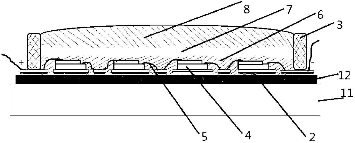
[0083] 3. Cut the above substrate to form a single packaged ceramic substrate, specifically including the aluminum substrate 11, Bi 2 o 3 Added ZnO pressure-sensitive ceramic film 12, copper / silver double-layer film electrode 2.

[0084] 4. Bond the LED bracket including metal heat sink 14 , lead pin 15 , and molding compound 16 on the above-mentioned substrate with silver glue 13 .

[0085] 5. Bake in the oven for 2 hours at 120 oC. Let cool, and take out when the temperature drops to room temperature.

[0086] 6. Weld the lead pin 15 on the positive and negative electrodes 3 .

[0087] 7. Solder the LED chip 4 to the pin 15 wi...


PUM

PropertyMeasurementUnit
thicknessaaaaaaaaaa
thicknessaaaaaaaaaa
particle diameteraaaaaaaaaa

Abstract

The invention belongs to the technical field of LED (light emitting diode) light sources, in particular to an LED packaged on a ZnO-based voltage-sensitive composite ceramic substrate. The LED comprises a radiating substrate, electrostatic protection material, an LED chip, a gold wire connection line, fluorescent powder and silica gel, wherein the radiating substrate adopts a ZnO pressure-sensitive composite ceramic substrate and the like; the ZnO pressure-sensitive composite ceramic is prepared by adding second phase nanometer high thermal conductivity ceramic materials such as Bi2O3 in matrix ceramic and sintering the mixture. In the invention, the high thermal conductivity ceramic material is adopted to add into ZnO ceramic matrix material, so as to form a network, realize a high thermal conductivity network heat conduction route, and reduce the LED thermal resistance of the ceramic material packaging; and a plurality of similar zener didoes which are in positive and negative series connections are formed, so as to realize high resistance and electrostatic function. The LED manufactured by the invention is simple in packaging structure, small in thermal resistance, high efficient, good in resistance to light fade, low in cost, strong in antistatic capability, and is suitable for being used for manufacturing low cost, high efficiency and high power LEDs.

Description

technical field [0001] The invention belongs to the technical field of LED light sources, and specifically relates to a light-emitting diode (LED) and a preparation method thereof, more specifically, to an LED packaged on a zinc oxide-bismuth oxide composite ceramic substrate and a preparation method thereof. Background technique [0002] Since the Japanese scientist Nakamura Shuji invented the commercial nitride blue light-emitting diode (LED) in 1993, the research and application of LED have developed rapidly. Among them, semiconductor solid-state lighting based on high-power white LED technology has high electro-optical conversion efficiency, long life, safety, and environmental protection, and is favored by governments all over the world. Internationally, the United States Department of Energy has formulated a solid-state lighting plan; Japan formulated the "21st Century Lighting Plan" in 1998; the European Union formulated the "Rainbow Project" in 2000, etc., actively p...

Claims


Application Information

Patent Timeline
Patent Type & Authority Applications(China)
IPC IPC(8): H01L33/48H01L33/64H01L25/075H01L23/60
CPCH01L2924/181H01L2224/45144H01L2224/48091H01L2224/48247H01L2224/49107H01L2924/00014H01L2924/00H01L2924/00012
Inventor 崔旭高龙天光张静莫晓亮黄高山梅永丰
Owner 泰州市华强照明器材有限公司
Why Eureka
Try Eureka