Thin film transistor, manufacturing method therefor, and display apparatus having thin film transistor, sputtering target material
A technology for thin film transistors and sputtering targets, which is used in transistors, semiconductor/solid-state device manufacturing, identification devices, etc., can solve the problems of difficult etching of laminated structures and increased manufacturing costs, and achieve good adhesion and electrical characteristics. The effect of reducing the realization and suppressing the diffusion of
- Summary
- Abstract
- Description
- Claims
- Application Information
AI Technical Summary
Problems solved by technology
Method used
Image

Examples
Embodiment 1
[0126]
[0127] Hereinafter, a method of manufacturing the TFT of Example 1 will be described. The semiconductor layer of the TFT of the first embodiment is composed of a silicon film, and in the bottom gate type, it has a top contact structure in which a source electrode and a drain electrode are formed after the semiconductor layer is formed. In addition, since the TFT structure becomes complicated when reflecting the correct film thickness and size, the figure is a schematic representation.
[0128] Figure 8 It is a figure showing the manufacturing process of the TFT of this Example, Figure 8 (a) to (d) are cross-sectional views of the TFT during the respective steps.
[0129] First, a Cu alloy 2 is formed into a film by sputtering or the like on a substrate 1 made of an insulating material such as alkali-free glass. The film thickness of the Cu alloy 2 is, for example, about 10 nm to 150 nm, preferably 20 nm to 50 nm. Here, the Cu alloy 2 to be deposited has a func...
Embodiment 1 and 2~19
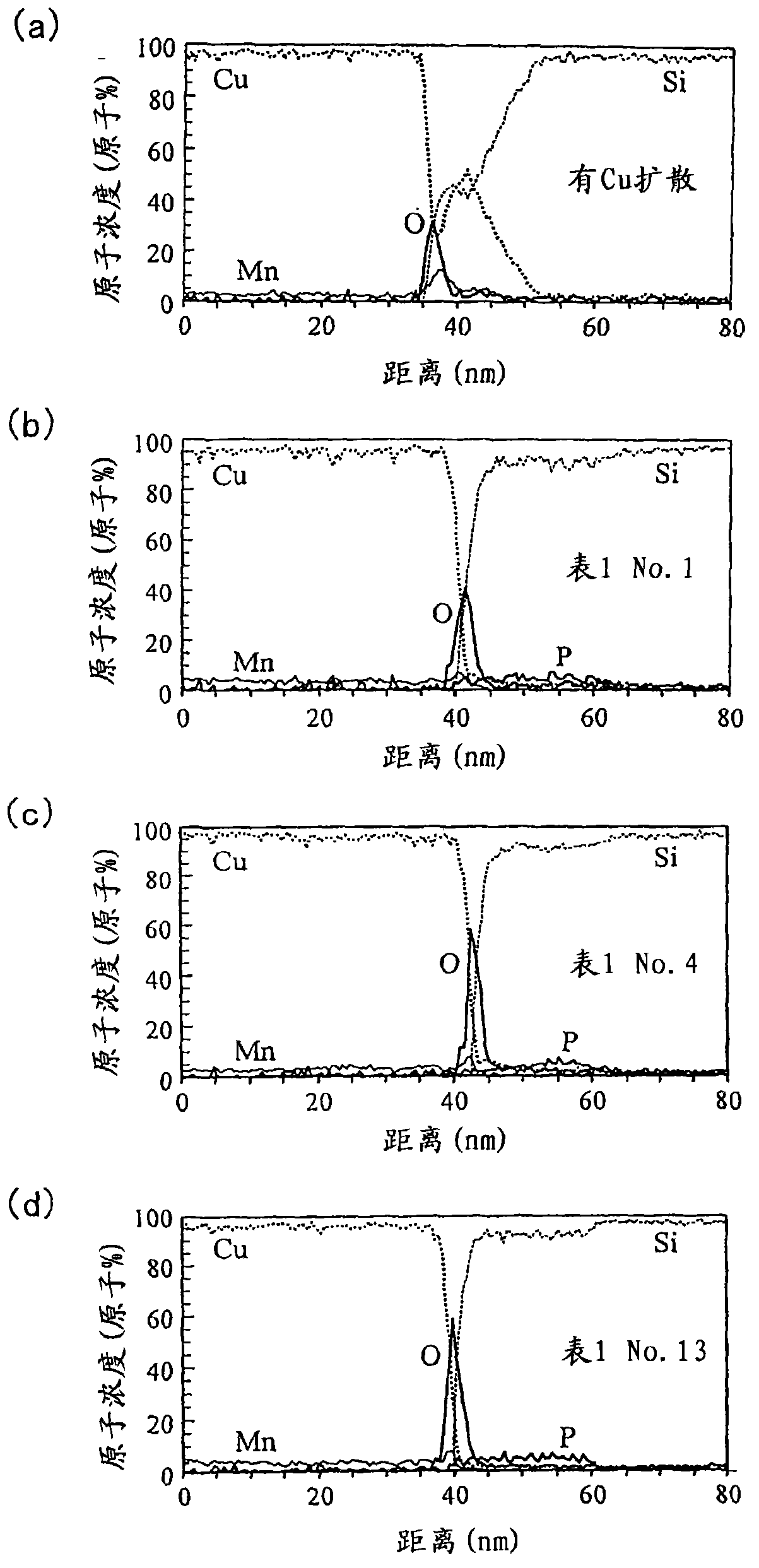
[0143] As shown in Table 2, in Example 1, the element added to the copper alloy electrode was Mo, but in Examples 2 to 19, the components and addition concentrations in Table 2 were used respectively, and the same as in Example 1 In the same manner, a copper alloy electrode having the composition and target addition concentration shown in Table 2 was formed into a thin film transistor. The actual concentration of additive elements in the source / drain copper alloy electrodes is quantified by taking out the substrate during the manufacturing process and using EDX (Energy Dispersive X-ray Spectroscopy). The manufactured thin film transistor was left in the atmosphere at 25° C. for 60 days, and the presence or absence of peeling of the Si semiconductor layer and the source / drain copper alloy electrode was investigated by a scanning electron microscope. In addition, the presence or absence of etching residues when the source / drain copper alloy electrodes were formed by etching in t...
Embodiment 20
[0149]
[0150] Hereinafter, a method of manufacturing a TFT according to Example 20 of the present invention will be described. The semiconductor layer of the TFT of Example 20 is composed of an oxide semiconductor film, and has a top contact structure in which a source electrode and a drain electrode are formed after the semiconductor layer is formed in the bottom gate type. In addition, since the TFT structure becomes complicated when reflecting the correct film thickness and size, it is shown schematically in the drawing. In addition, a part of the repeated description in the second embodiment and the first embodiment is omitted.
[0151] Figure 10 (a)-(d) are figures which show the cross-section of TFT in each process. First, as in Example 1, a Cu alloy 2 is formed (deposited) by a sputtering method on a substrate 1 made of an insulating material such as alkali-free glass. Next, pure Cu 3 is continuously deposited (deposited) by the same sputtering method. After pe...
PUM
| Property | Measurement | Unit |
|---|---|---|
| Film thickness | aaaaa | aaaaa |
| Film thickness | aaaaa | aaaaa |
Abstract
Description
Claims
Application Information
 - Generate Ideas
- Intellectual Property
- Life Sciences
- Materials
- Tech Scout
- Unparalleled Data Quality
- Higher Quality Content
- 60% Fewer Hallucinations
Browse by: Latest US Patents, China's latest patents, Technical Efficacy Thesaurus, Application Domain, Technology Topic, Popular Technical Reports.
© 2025 PatSnap. All rights reserved.Legal|Privacy policy|Modern Slavery Act Transparency Statement|Sitemap|About US| Contact US: help@patsnap.com