Manufacture method for monolithic integration titanium film thermal resistor tunable distributed feed back (DFB) laser

A DFB laser and manufacturing method technology, which is applied to lasers, laser parts, semiconductor lasers, etc., can solve problems such as complex processes, and achieve the effect of simplifying the manufacturing process and reducing the manufacturing cost.

Active Publication Date: 2013-05-08
INST OF SEMICONDUCTORS - CHINESE ACAD OF SCI
View PDF2 Cites 4 Cited by
  • Summary
  • Abstract
  • Description
  • Claims
  • Application Information

AI Technical Summary

Problems solved by technology

Almost all researchers use platinum metal to make thin-film resistors, but since platinum metal does not have a corresponding etching solution to make thin-film resistor strip patterns, it is necessary to use techniques such as lift

Method used


Image

  • Manufacture method for monolithic integration titanium film thermal resistor tunable distributed feed back (DFB) laser
  • Manufacture method for monolithic integration titanium film thermal resistor tunable distributed feed back (DFB) laser
  • Manufacture method for monolithic integration titanium film thermal resistor tunable distributed feed back (DFB) laser

Examples


Embodiment 1

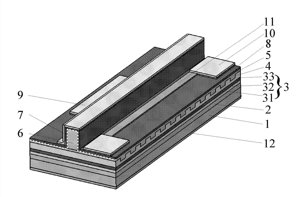
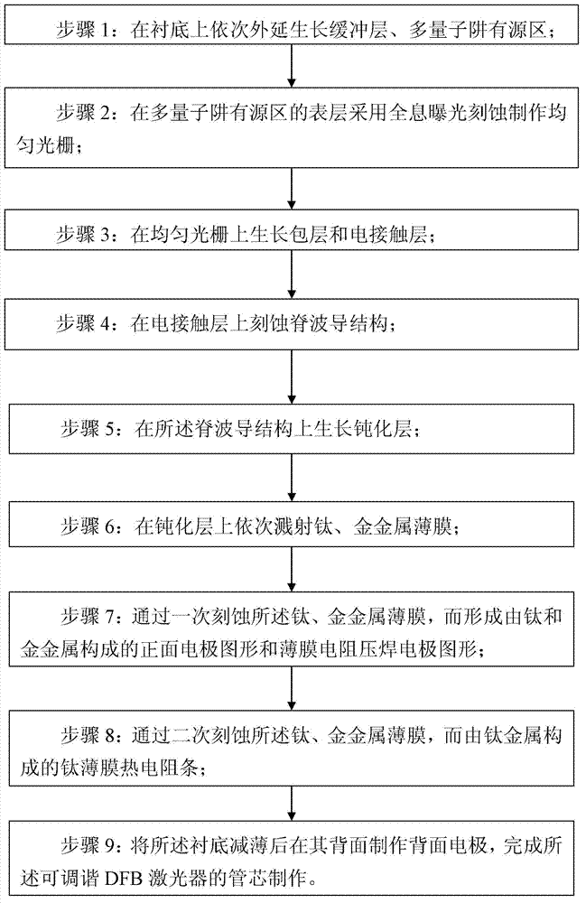
[0042] In a preferred embodiment of the present invention, the manufacturing method of the N-type substrate monolithically integrated titanium thin film thermal resistance tunable DFB laser comprises the following steps:

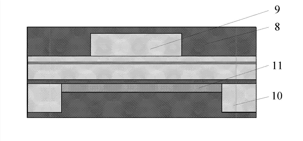
[0043] Select an N-type indium phosphide substrate 1 with a doping concentration of 5×10 17 cm -3 , the crystal plane is (100); the buffer layer 2, the multi-quantum well active region 3 and the electrical contact layer 4 are epitaxially grown sequentially on the N-type indium phosphide substrate 1, and the multi-quantum well active region 3 includes sequentially grown The lower waveguide layer 31, the core layer 32 and the upper waveguide layer 33; the material of the core layer 32 in the multi-quantum well active region 3 is InGaAsP, with a thickness of 70 nanometers.

[0044] Fabricate a uniform grating 4 on the surface layer of the multi-quantum well active region 3; grow a cladding layer 5 and an electrical contact layer 6 on the uniform grating 4; use...

Embodiment 2

[0048] In another preferred embodiment of the present invention, the manufacturing method of the N-type substrate monolithically integrated titanium thin film thermal resistance tunable DFB laser comprises the following steps:

[0049] Select an N-type indium phosphide substrate 1 with a doping concentration of 5×10 18 cm -3 , the crystal plane is (100); the buffer layer 2, the multi-quantum well active region 3 and the electrical contact layer 4 are epitaxially grown sequentially on the N-type indium phosphide substrate 1, and the multi-quantum well active region 3 includes sequentially grown The lower waveguide layer 31, the core layer 32 and the upper waveguide layer 33; the material of the core layer 32 in the multi-quantum well active region 3 is InGaAsP, with a thickness of 120 nanometers.

[0050] Fabricate a uniform grating 4 on the surface layer of the multi-quantum well active region 3; grow a cladding layer 5 and an electrical contact layer 6 on the uniform grating...

Embodiment 3

[0054] In another preferred embodiment of the present invention, the manufacturing method of the N-type substrate monolithically integrated titanium thin film thermal resistance tunable DFB laser comprises the following steps:

[0055] Select an N-type indium phosphide substrate 1 with a doping concentration of 2×10 18 cm -3 , the crystal plane is (100); the buffer layer 2, the multi-quantum well active region 3 and the electrical contact layer 4 are epitaxially grown sequentially on the N-type indium phosphide substrate 1, and the multi-quantum well active region 3 includes sequentially grown The lower waveguide layer 31, the core layer 32 and the upper waveguide layer 33; the material of the core layer 32 in the multi-quantum well active region 3 is InGaAsP, with a thickness of 100 nanometers.

[0056] Fabricate a uniform grating 4 on the surface layer of the multi-quantum well active region 3; grow a cladding layer 5 and an electrical contact layer 6 on the uniform grating...


PUM

PropertyMeasurementUnit
Doping concentrationaaaaaaaaaa
Thicknessaaaaaaaaaa
Thicknessaaaaaaaaaa

Abstract

The invention discloses a manufacture method for a monolithic integration titanium film thermal resistor tunable distributed feed back (DFB) laser. The manufacture method comprises the steps of selecting an indium phosphide substrate 1, sequentially and epitaxially growing a buffer layer 2 and a multiple quantum wells active area 3 on the substrate 1, manufacturing even gratings 4 on the surface layer of the multiple quantum wells active area 3 by adopting holographic exposure etching, growing a cladding 5 and an electric contact layer 6 on the even gratings 4, adopting a regular photoetching and etching process, manufacturing a ridge waveguide structure 7 on the electric contact layer 6, growing a passivation layer 8 on the manufactured ridge waveguide structure 7, sputtering titanium and gold metal film on the passivation layer 8 after a front face electrode window is opened by adopting regular photoetching, coating photoresist on the metal film, photoetching a front face electrode pattern 9, a film resistor pressure welding electrode pattern 10 and a film resistor area 11 for once, photoetching and selectively etching for twice to form a titanium film thermal resistor strip 11, manufacturing a back face electrode 12 on the back face of the substrate 1 after the indium phosphide substrate 1 is thinned, and achieving manufacturing of a tube core.

Description

technical field [0001] The invention relates to the field of optoelectronic devices, in particular to a method for manufacturing a monolithic integrated titanium thin film thermal resistance tunable DFB laser. Background technique [0002] In modern high-speed optical communication systems, wavelength tunable lasers are key devices in optical communication networks and systems. It currently has a wide range of application market prospects, such as atmospheric monitoring, measurement, sensing and other fields. In addition, it is a key component in high-speed and large-capacity optical communication systems, wavelength division multiplexing, and time division multiplexing systems. light source. [0003] Semiconductor Distributed Feedback (DFB) laser has excellent dynamic single longitudinal mode characteristics, mature manufacturing process, stable device performance and high reliability. It is currently the most important light source for optical fiber communication systems...

Claims


Application Information

Patent Timeline
IPC IPC(8): H01S5/026H01S5/12
Inventor 张灿梁松朱洪亮
Owner INST OF SEMICONDUCTORS - CHINESE ACAD OF SCI
Why Eureka
Try Eureka