Method for preparing graphene film on nonmetallic substrate at low temperature

A graphene thin film, non-metallic technology, applied in the field of graphene thin film preparation, can solve the problems that are not suitable for optoelectronic device construction and industrial production application, difficult to realize graphene growth, increase power consumption and time cost, and achieve the preparation process Energy saving, low defect density, reduced application effect

Inactive Publication Date: 2013-07-10
满锦梦
View PDF6 Cites 17 Cited by
  • Summary
  • Abstract
  • Description
  • Claims
  • Application Information

AI Technical Summary

Problems solved by technology

[0009] Although the conventional chemical vapor deposition method provides an effective way to control the number and size of graphene layers, it is a pity that the preparation of graphene by conventional chemical vapor deposition generally requires catalytic growth of graphene on the metal surface. , and then transfer the metal to a different substrate after etching, and the growth temperature is as high as 1000 ° C or even higher, which increases power consumption and time costs, etc., and also puts forward higher requirements for equipment; in addition, the Mr. It is difficult to obtain a uniform high...

Method used


Image

  • Method for preparing graphene film on nonmetallic substrate at low temperature
  • Method for preparing graphene film on nonmetallic substrate at low temperature
  • Method for preparing graphene film on nonmetallic substrate at low temperature

Examples


Embodiment 1

[0046] A method for preparing graphene film at a low temperature on a non-metallic substrate, the non-metallic substrate being a silicon substrate, comprising the following steps:

[0047] In the first stage, first, cut the silicon substrate with a silicon dioxide film with a thickness of 300nm into small pieces of about 1cm in size, wash them with acetone and deionized water, and then put them in an oven to dry; then Use steps such as oxygen plasma cleaning and hydrogen high temperature treatment to remove residual impurities on the surface.

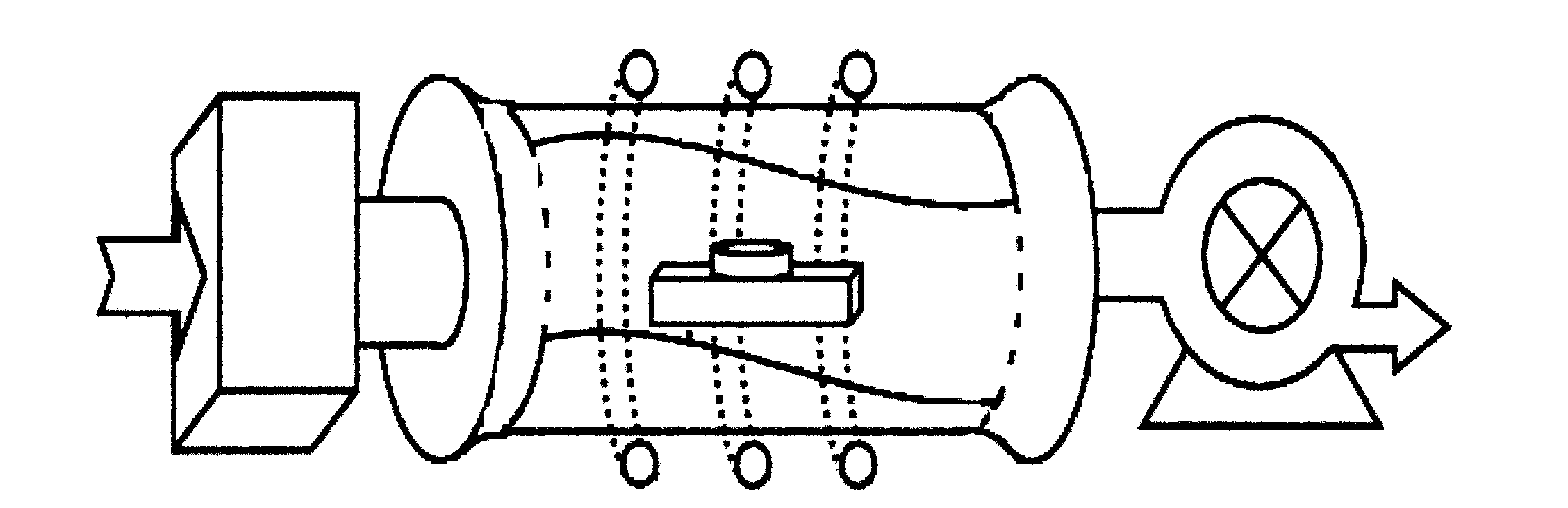
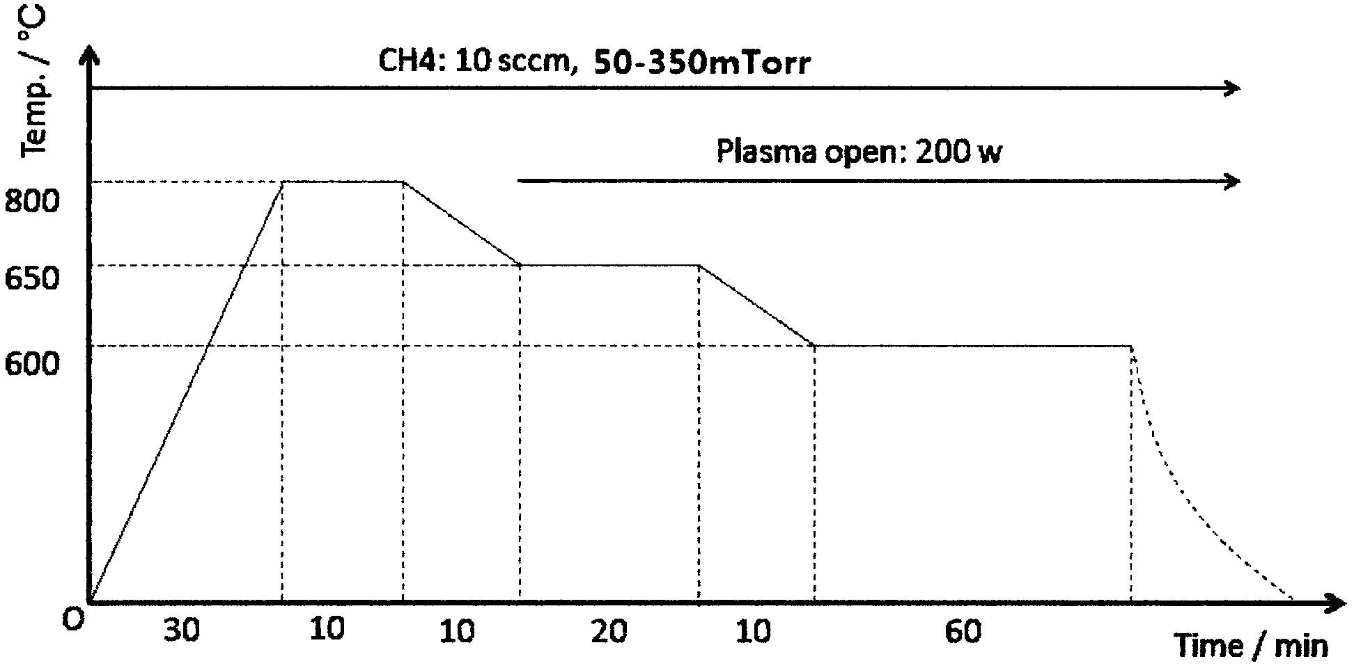
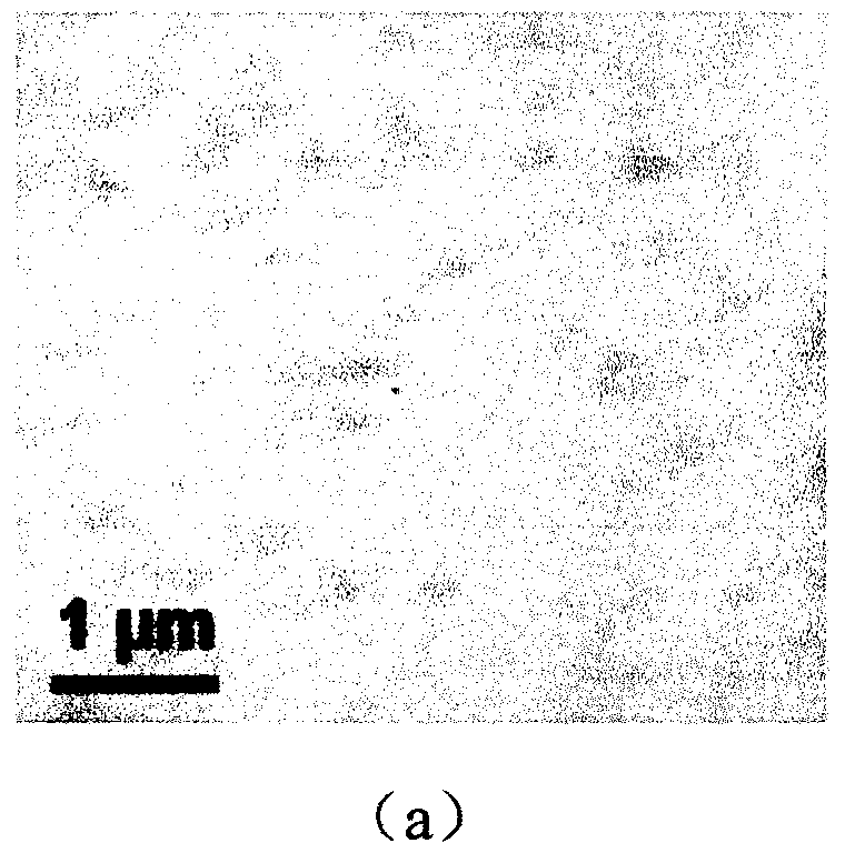
[0048] In the second stage, firstly, the processed silicon substrate is placed on the quartz glass plate, and then the quartz plate with the substrate is placed in such as figure 1 In the shown vacuum reaction furnace (the position of the quartz plate is close to the side of the plasma source, and deviates from the center of the reaction furnace by about 10cm); then, use a vacuum pump to pump the vacuum reaction furnace to a low pressur...

Embodiment 2

[0051] According to the preparation method of Example 1, the non-metallic substrate is changed to a sapphire substrate, and the substrate can be selected not to use oxygen plasma or high-temperature hydrogen for surface treatment, and the obtained graphene film is a multilayer film, and the film is relatively uniform.

Embodiment 3

[0053] According to the preparation method of Example 1, the non-metallic substrate is changed to a quartz substrate, and the substrate can be selected not to use oxygen plasma or high-temperature hydrogen for surface treatment, and the obtained graphene film is a multilayer film, and the film is relatively uniform.


PUM


Abstract

The invention discloses a method for preparing a graphene film on a nonmetallic substrate at low temperature. By adopting the method disclosed by the invention, a plasma source is introduced to the graphene film preparation process by using a technology of chemical vapor deposition method to prepare a uniform graphene film on the non-catalytic non-metallic substrate, the technology for preparing the graphene by means of traditional chemical vapor deposition method is improved, the direct growth of the graphene on the surface of a semiconductor base material and an insulator medium base material are achieved to realize target application, the shortcoming that the uniform and high-quality graphene film on a curved surface or a surface with a three-dimensional structure cannot be prepared by using the traditional method is overcome, and the subsequent necessary metal etching and graphene transfer steps during graphene preparation by the traditional chemical vapor deposition method are eliminated; as plasma enhancement effect is utilized, the method disclosed by the invention effectively reduces graphene preparation temperature, not only is energy saving, but also is practical, simultaneously, the method reduces working procedures, reduces cost, and has a pretty good application prospect in the aspects of preparing a transparent electrode material and constructing an electronic component and a photoelectron component.

Description

technical field [0001] The invention belongs to the technical field of graphene preparation, and in particular relates to a method for preparing a graphene film. Background technique [0002] With the rapid development of modern information technology, the shortcomings of silicon materials such as low electro-optic coefficient and low luminous efficiency hinder the application of silicon materials in the field of high-speed and high-bandwidth data transmission. The development has injected fresh blood. [0003] Dirac materials represented by graphene have been widely concerned by researchers from all over the world since their inception, and have become a new research hotspot. As a unique two-dimensional crystal, graphene has excellent mechanical properties, ultra-high thermal conductivity and carrier mobility, and relatively high carrier saturation drift velocity, making graphene widely used in transistors, solar cells, and sensors. , supercapacitors, ultrafast electronic...

Claims


Application Information

Patent Timeline
IPC IPC(8): C01B31/04C01B32/188
Inventor 鲍桥梁林生晃陈彩云袁建李鹏飞许梦
Owner 满锦梦
Why Eureka
Try Eureka