High-voltage-resistant and high-energy-density capacitor and preparation method thereof
A technology with high energy storage density and capacitors, applied in the direction of multilayer capacitors, fixed capacitor electrodes, fixed capacitor dielectrics, etc., can solve the problems of poor semiconductor integration process compatibility, large capacitor volume, and low capacitor energy storage density, etc., to achieve optimal orientation. and the effects of electrical properties, high energy storage density, and high-efficiency preparation
- Summary
- Abstract
- Description
- Claims
- Application Information
AI Technical Summary
Problems solved by technology
Method used
Image

Examples
Embodiment 1
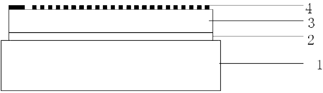
[0036] Heat the substrate to 200-500℃ through the heating wire, adjust the revolution motor so that the substrate is facing the Ti target, turn on the RF power of the Ti target, and adjust the power density of the Ti target to 2-5W / cm 2, a Ti metal film with a thickness of 20-100 nm was prepared as the transition layer between the electrode Pt and the Si matrix.
[0037] Adjust the revolution motor so that the substrate is in the position facing the Pt target, turn on the RF power supply of the Pt target, and adjust the power density of the Pt target to 2-5W / cm 2 , Pt metal films with a thickness of 80-500 nm were prepared.
[0038] Then, oxygen with a flow rate of 10-40sccm is introduced into the chamber, and the valve plate valve of the equipment is adjusted to keep the chamber pressure at 0.3-3pa. Adjust the revolution motor so that the substrate is facing the BaTiO 3 Target position, turn on BaTiO 3 Target RF power supply, tuned BaTiO 3 The power density of the target ...
Embodiment 2
[0041] All films were prepared at medium and low temperature (≤500°C).
[0042] Using a single target to perform radio frequency magnetron coaxial sputtering in sequence, including the following steps:
[0043] (i) Matrix treatment:
[0044] Choose Si or SiO 2 / Si was used as the substrate of the film capacitor, which was ultrasonically cleaned with acetone and alcohol and dried by blowing. Heat it to 200-500°C.
[0045] (ii) Deposition of metal thin films on the substrate:
[0046] Using metal Ti target and Pt target, it is completed by radio frequency magnetron sputtering. The sputtering atmosphere is pure Ar, the gas flow is controlled at 20-100sccm, the gas pressure is 0.3-3Pa, and the target power density is 2-5W / cm 2 , the total film thickness is controlled at 100-600nm.
[0047] (iii) Deposition of conductive oxide films:
[0048] Using perovskite LaNiO 3 The target is completed by radio frequency magnetron sputtering. The sputtering atmosphere is Ar and O 2 ,...
PUM
| Property | Measurement | Unit |
|---|---|---|
| Thickness | aaaaa | aaaaa |
| Thickness | aaaaa | aaaaa |
| Diameter | aaaaa | aaaaa |
Abstract
Description
Claims
Application Information