Copper metal connection line of three-five compound semiconductor assembly

A copper metal and compound technology, applied in semiconductor devices, semiconductor/solid-state device components, electric solid-state devices, etc., can solve the problem that compound semiconductors cannot be directly applied, and achieve the effect of reducing production costs

Inactive Publication Date: 2013-08-21
WIN SEMICON
View PDF7 Cites 2 Cited by
  • Summary
  • Abstract
  • Description
  • Claims
  • Application Information

AI Technical Summary

Problems solved by technology

In semiconductor integrated circuits mainly based on silicon components, many technological inventions have been made in the copper metallization process; however, these technologies cannot be directly applied to the compound semiconductor manufacturing process

Method used


Image

  • Copper metal connection line of three-five compound semiconductor assembly
  • Copper metal connection line of three-five compound semiconductor assembly
  • Copper metal connection line of three-five compound semiconductor assembly

Examples


Embodiment Construction

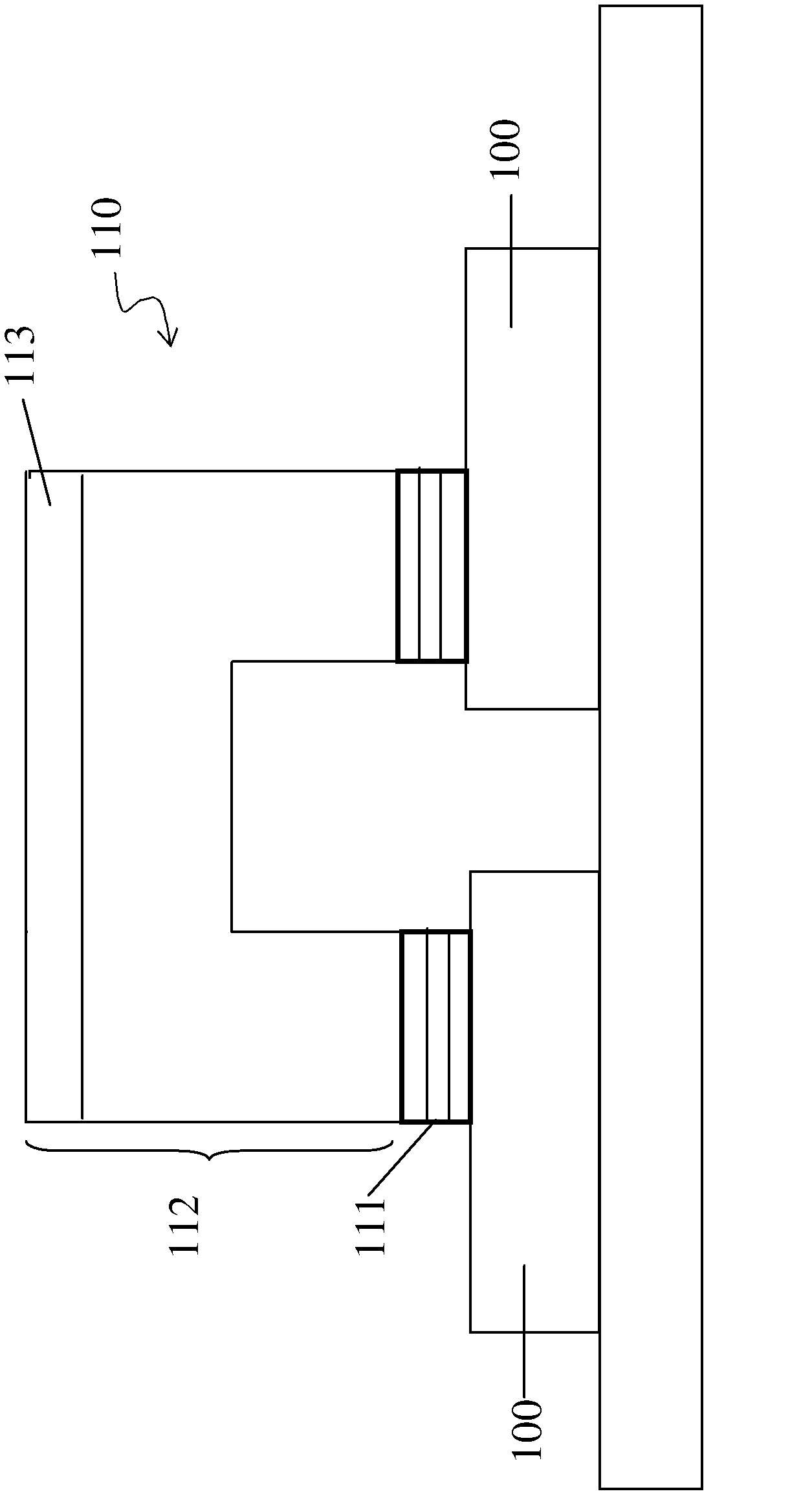
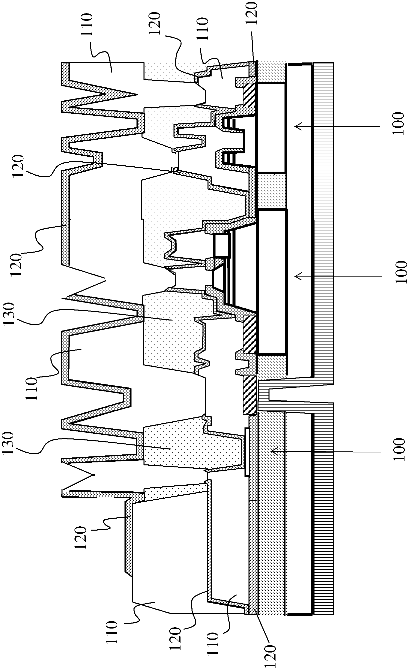
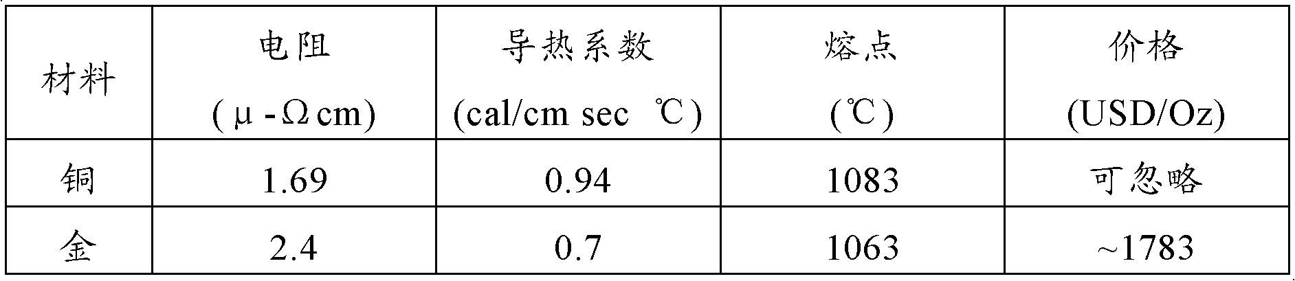
[0017] figure 1 It is a schematic cross-sectional structure diagram of a copper metal connection wire of a III-V compound semiconductor component of the present invention, including a III-V compound semiconductor component 100, wherein the III-V compound semiconductor component is made of gallium arsenide (GaAs), indium phosphide ( InP) or gallium nitride (GaN) and other III-V compound semiconductor materials; the III-V compound semiconductor component can be a heterojunction bipolar transistor (HBT), a heterojunction field effect transistor ( HFET), a diode or other III-V compound semiconductor components; and a copper metal connection line 110; the copper metal connection line 110 includes a metal contact layer 111 and a copper-containing metal layer 112; the metal contact layer 111 is located on the copper-containing Below the metal layer 112, an adhesion layer is used to adhere to the semiconductor material below; a barrier layer is used to isolate the diffusion of copper ...


PUM

PropertyMeasurementUnit
Thicknessaaaaaaaaaa
Thicknessaaaaaaaaaa
Thicknessaaaaaaaaaa

Abstract

The invention discloses a copper metal connection line of a three-five compound semiconductor assembly. The copper metal connection line comprises a metal contact layer and a copper-bearing metal layer, wherein the metal contact layer is arranged below the copper-bearing metal layer. The copper metal connection line is made of a group chosen by the following materials: titanium, palladium and copper (Ti, Pd and Cu), titanium, vanadium and copper (Ti, NiV and Cu), tungsten, titanium nitride tungsten, tungsten and copper (TiW, TiWn, TiW and Cu), tungsten, titanium nitride tungsten, tungsten and aurum (TiW, TiWN, TiW and Au), tungsten and copper (TiW and Cu), and tungsten and aurum (TiW and Au). The copper-bearing metal layer further comprises a metal protective layer which covers above the copper-bearing metal layer, wherein the metal protective layer is used for preventing the copper-bearing metal layer from being oxidized. The metal protective layer is made of nickel and aurum (Ni and Au) or nickel, palladium and aurum (Ni, Pd and Au) or a solder.

Description

technical field [0001] The invention relates to a copper metal connecting wire of a semiconductor component, in particular to a copper metal connecting wire of a III-V compound semiconductor component. Background technique [0002] Traditionally, due to the high stability of gold, in the front-end process of compound semiconductor integrated circuits, metal connection lines are mostly composed of metal layers containing gold. However, the high price of gold has become one of the bottlenecks for the compound semiconductor industry to control production costs; in terms of application, the demand for integrated circuits tends to be higher integration and higher efficiency, so lower resistance and better heat dissipation efficiency are required wire material. As shown in Table 1, compared with gold, copper as a wire material has lower resistance value, better heat dissipation rate, higher thermal stability, and most importantly, its price is much lower than gold. Therefore, if ...

Claims


Application Information

Patent Timeline
IPC IPC(8): H01L23/532
Inventor 花长煌朱文慧
Owner WIN SEMICON
Why Eureka
Try Eureka