

Patterned composite ceramic layer printed wiring substrate for optical and electronic devices
A technology of composite ceramics and electronic devices, applied in the field of electronics, can solve problems such as difficult heat transfer, electrical conduction short circuit, etc., and achieve the effects of solving heat dissipation problems, good electrical isolation and thermal isolation, and high withstand voltage breakdown performance.
- Summary
- Abstract
- Description
- Claims
- Application Information
AI Technical Summary
Problems solved by technology
Method used
Image

Examples
Embodiment 1
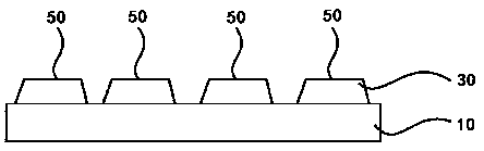
[0025] as attached figure 1 As shown, the patterned composite ceramic layer printed circuit board for optical and electronic devices described in this embodiment includes an aluminum or aluminum alloy substrate 10 on which a pressure-resistant and high-thermal-conduction substrate is formed. and the composite ceramic layer 30 is selectively etched through a mask to form a plurality of isolation bases 50; and a metal circuit layer (not shown in the figure) is formed on the isolation bases. The step of the composite pressure-resistant ceramic layer adopts the following process, and its reaction system is AlCl 3 -H 2 O-NH 3 -O 2 -H 2 , the reaction temperature is 420-450°C, the working pressure is 1200Pa, where AlCl 3 The flow rate is 50ml / min, H 2 The flow rate of O is 10-20ml / min, O 2 The flow rate is 15-20ml / min, NH 3 The flow rate is 25-30ml / min, H 2 The flow rate is 500ml / min, and the film thickness is 200μm. The breakdown voltage of the structure obtained by this ...
Embodiment 2
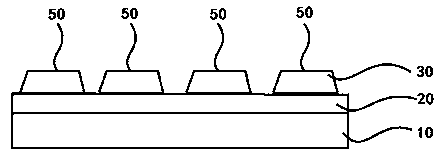
[0027] as attached figure 2 As shown, the patterned composite ceramic layer printed circuit board for optical and electronic devices described in this embodiment includes an aluminum or aluminum alloy substrate 10 on which a pressure-resistant and high-thermal-conduction substrate is formed. A composite ceramic layer 30; an aluminum transition layer 20 is provided between the aluminum or aluminum alloy substrate 10 and the composite ceramic layer 30, and the composite ceramic layer 30 is selectively etched through a mask to form a plurality of isolation bases 50; And a metal circuit layer (not shown in the figure) is formed on the isolation base. Wherein, the step of the aluminum transition layer adopts the following process: vacuumize to 5.0×10 - 4 Pa, into the vacuum coating chamber with a purity of 99.99% Ar, a flow rate of 20sccm, and keep the working vacuum in the vacuum coating chamber at 50Pa, turn on a pair of intermediate frequency sputtering power supplies with al...
Embodiment 3
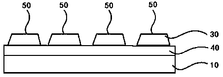
[0029] as attached image 3 As shown, the patterned composite ceramic layer printed circuit board for optical and electronic devices described in this embodiment includes a copper or copper alloy substrate 10, and a pressure-resistant and high thermal conductivity substrate is formed on the copper or copper alloy substrate 10. There is an active brazing layer 40 between the copper or copper alloy substrate 10 and the composite ceramic layer 30, and the composite ceramic layer 30 is selectively etched through a mask to form a plurality of isolation bases 50 ; and a metal circuit layer (not shown in the figure) is formed on the isolation base. The composite ceramic layer is composed of beryllium oxide and aluminum oxide. The composite ceramic layer is made by powder sintering method, the sintering temperature is 1850-2000° C., and the thickness of the composite ceramic layer is 200 μm. The composite ceramic layer is bonded to the surface of the copper or copper alloy substrate ...
PUM
| Property | Measurement | Unit |
|---|---|---|
| thickness | aaaaa | aaaaa |
| thickness | aaaaa | aaaaa |
| thickness | aaaaa | aaaaa |
Abstract
Description
Claims
Application Information