Preparation method for depositing InN film on GaN buffer layer/diamond film/Si multilayer film structure substrate at low temperature by ECR-PEMOCVD (electron cyclotron resonance-plasma-enhanced metal-organic chemical vapor deposition)

A diamond thin film and buffer layer technology, which is applied in coating, metal material coating process, gaseous chemical plating, etc., can solve the problems of difficulty in reducing device cost, hindering the development of InN material devices, and high price of sapphire substrates. Effects of lattice mismatch, low cost, good electrical and thermal performance

Active Publication Date: 2013-10-23
辽宁众城新能源开发有限公司
View PDF2 Cites 1 Cited by
  • Summary
  • Abstract
  • Description
  • Claims
  • Application Information

AI Technical Summary

Problems solved by technology

As we all know, the price of sapphire substrate is relatively high. Using it as the substrate of InN material makes it...

Method used


Image

  • Preparation method for depositing InN film on GaN buffer layer/diamond film/Si multilayer film structure substrate at low temperature by ECR-PEMOCVD (electron cyclotron resonance-plasma-enhanced metal-organic chemical vapor deposition)
  • Preparation method for depositing InN film on GaN buffer layer/diamond film/Si multilayer film structure substrate at low temperature by ECR-PEMOCVD (electron cyclotron resonance-plasma-enhanced metal-organic chemical vapor deposition)
  • Preparation method for depositing InN film on GaN buffer layer/diamond film/Si multilayer film structure substrate at low temperature by ECR-PEMOCVD (electron cyclotron resonance-plasma-enhanced metal-organic chemical vapor deposition)

Examples


Embodiment 1

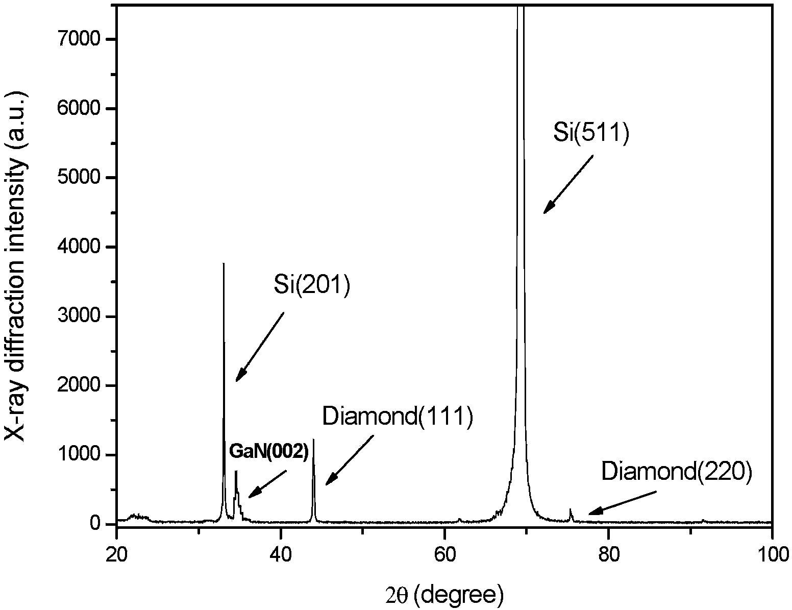
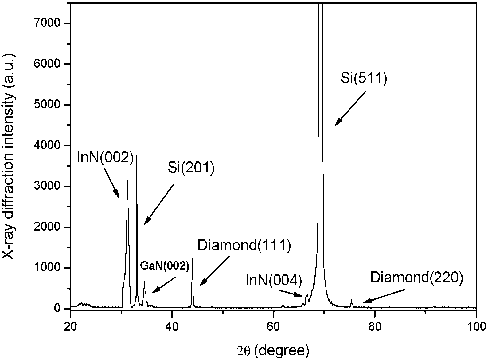
[0041] After the Si substrate was ultrasonically cleaned with acetone, ethanol and deionized water for 5 minutes, it was blown dry with nitrogen and sent to the reaction chamber; the reaction chamber was evacuated to 1.0×10 with a hot wire CVD system. -2 Pa, the substrate is heated to 800°C, and hydrogen and methane gas are introduced into the reaction chamber. The flow rate of the two is 200 sccm for hydrogen and 4 sccm for methane, controlled by a mass flow meter; the voltage of the hot wire is 10V, and the current of the filament is 50A. After reacting for 30 minutes, a diamond film was obtained on the Si substrate. ECR-PEMOCVD system was used to evacuate the reaction chamber to 8.0×10 -4 Pa, the substrate is heated to 400°C, trimethylgallium and nitrogen carried by hydrogen gas are introduced into the reaction chamber, and the flow rates of the two are 0.5 sccm and 100 sccm respectively, controlled by a mass flow meter; the total pressure of the control gas is ...

Embodiment 2

[0044] After the Si substrate was ultrasonically cleaned with acetone, ethanol and deionized water for 5 minutes, it was blown dry with nitrogen and sent to the reaction chamber; the reaction chamber was evacuated to 1.0×10 with a hot wire CVD system. -2 Pa, the substrate is heated to 800°C, and hydrogen and methane gas are introduced into the reaction chamber. The flow rate of the two is 200 sccm for hydrogen and 4 sccm for methane, controlled by a mass flow meter; the voltage of the hot wire is 10V, and the current of the filament is 50A. After reacting for 30 minutes, a diamond film was obtained on the Si substrate. ECR-PEMOCVD system was used to evacuate the reaction chamber to 8.0×10 -4 Pa, the substrate is heated to 200°C, trimethylgallium and nitrogen carried by hydrogen gas are introduced into the reaction chamber, and the flow rates of the two are 0.5 sccm and 100 sccm respectively, controlled by a mass flow meter; the total pressure of the control gas is ...

Embodiment 3

[0046] After the Si substrate was ultrasonically cleaned with acetone, ethanol and deionized water for 5 minutes, it was blown dry with nitrogen and sent to the reaction chamber; the reaction chamber was evacuated to 1.0×10 with a hot wire CVD system. -2 Pa, the substrate is heated to 800°C, and hydrogen and methane gas are introduced into the reaction chamber. The flow rate of the two is 200 sccm for hydrogen and 4 sccm for methane, controlled by a mass flow meter; the voltage of the hot wire is 10V, and the current of the filament is 50A. After reacting for 30 minutes, a diamond film was obtained on the Si substrate. ECR-PEMOCVD system was used to evacuate the reaction chamber to 8.0×10 -4 Pa, the substrate is heated to 300°C, trimethylgallium and nitrogen carried by hydrogen gas are introduced into the reaction chamber, and the flow rates of the two are 0.5 sccm and 100 sccm respectively, controlled by a mass flow meter; the total pressure of the control gas is ...


PUM


Abstract

The invention belongs to the technical field of deposition preparation of novel photoelectric materials, and provides a preparation method for depositing an InN film on a GaN buffer layer/diamond film/Si multilayer film structure substrate at low temperature by ECR-PEMOCVD (electron cyclotron resonance-plasma-enhanced metal-organic chemical vapor deposition), which can prepare an InN photoelectric film with favorable electric properties at low cost. The invention comprises the following steps: 1) carrying out ultrasonic cleaning on an Si substrate sequentially with acetone, ethanol and deionized water, drying the Si substrate by blowing nitrogen, and sending into a reaction chamber; 2) by using a hot wire CVD (chemical vapor deposition) system, vacuumizing the reaction chamber, heating the Si substrate, and introducing hydrogen and methane gas into the reaction chamber to obtain a diamond film on the Si substrate; and 3) by using an ECR-PEMOCVD system, vacuumizing the reaction chamber, heating the substrate to 200-600 DEG C, and introducing hydrogen-carried trimethyl gallium and nitrogen into the reaction chamber.

Description

technical field [0001] The invention belongs to the technical field of deposition and preparation of new photoelectric materials, and in particular relates to a preparation method for low-temperature deposition of an InN thin film on a GaN buffer layer / diamond thin film / Si multilayer film structure substrate by ECR-PEMOCVD. Background technique [0002] Indium nitride (InN) is an important member of group III nitrides. Compared with GaN and AlN, InN has the highest mobility and peak rate, and has unique advantages in the application of high-speed and high-frequency transistors and other electronic devices. ; Its room temperature band gap is located in the near-infrared region, and it is also suitable for preparing optoelectronic devices such as high-efficiency solar cells, semiconductor light-emitting diodes, and optical communication devices. However, due to the low decomposition temperature of InN, a low growth temperature is required, and the decomposition temperature of ...

Claims


Application Information

Patent Timeline
IPC IPC(8): C23C16/34C23C16/511C23C16/27
Inventor 王存旭孙笑雨张宏丽王晓文许鉴李乃忠张玉艳王刚杜士鹏王胜辉
Owner 辽宁众城新能源开发有限公司
Why Eureka
Try Eureka