Femtosecond laser direct writing sapphire ring light guide and preparation method thereof

A femtosecond laser and sapphire technology, applied in the field of optoelectronics, can solve the problems of narrow transmission spectrum, poor mechanical strength and complexity, and achieve the effects of easy optical system integration, high temperature resistance transmission spectrum, and overcoming complex processes

Inactive Publication Date: 2013-11-20
XIDIAN UNIV
View PDF5 Cites 24 Cited by
  • Summary
  • Abstract
  • Description
  • Claims
  • Application Information

AI Technical Summary

Problems solved by technology

In this method, two high-purity quartz glass substrate tubes with different inner and outer diameters are used to construct optical fiber preforms and vapor phase chemical deposition (MCVD). The barrier layer and the fiber core layer are deposited in the annular area between the pure quartz sleeves. After the vapor deposition is completed, the outer sleeve is removed to shrink the inner high-purity quartz sleeve separately; the disadvantage of this patent application is that it cannot The length of the prepared ring waveguide is precisely controlled, and at the same time, due to the use of a complex vapor phase chemical deposition process (MCVD), the difficulty of the manu

Method used


Image

  • Femtosecond laser direct writing sapphire ring light guide and preparation method thereof
  • Femtosecond laser direct writing sapphire ring light guide and preparation method thereof
  • Femtosecond laser direct writing sapphire ring light guide and preparation method thereof

Examples


Embodiment Construction

[0037] The present invention will be further described below in conjunction with the accompanying drawings.

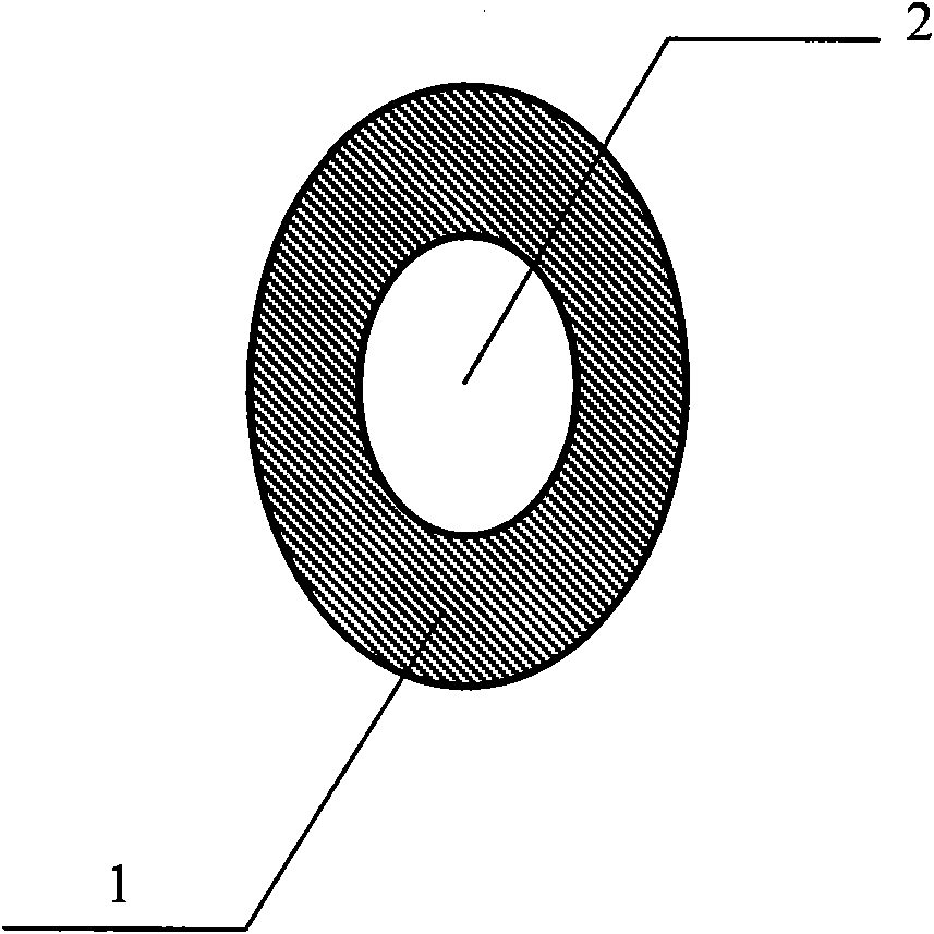
[0038] Refer to attached figure 1 , The femtosecond laser direct writing sapphire ring light guide area 1 of the present invention is a three-dimensional ring within 200nm adjacent to the femtosecond laser active area 2, and the cross section of the waveguide of the present invention is ellipsoidal.

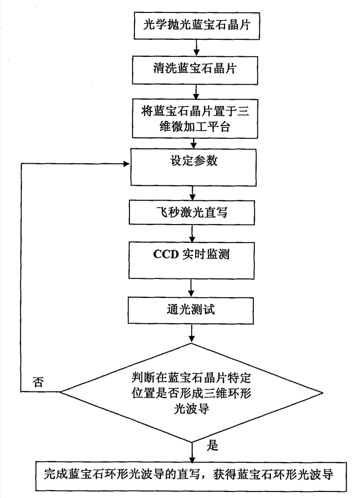
[0039] Refer to attached figure 2 , to further describe the implementation method of the present invention.

[0040] Step 1, optically polish the sapphire wafer.

[0041] Optically polishing square or round sapphire wafers with a thickness of 1-2 mm and a purity >96% to obtain a sapphire wafer with a flatness of <10 μm, a polished surface roughness of Ra <0.3 nm and a curvature of <10 μm. In the embodiment of the present invention, a square sapphire wafer with a thickness of 1mm and a purity of 99.9% is used. The polished flatness is 7 μm, the roughness is 0.2 nm, and...


PUM

PropertyMeasurementUnit
Thicknessaaaaaaaaaa

Abstract

The invention discloses a femtosecond laser direct writing sapphire ring light guide and a preparation method thereof. A cross section of the prepared femtosecond laser direct writing sapphire ring light guide is elliptic, a light guide part thereof is in a shape of a three-dimensional ring, which is close to a femtosecond laser acting region, and the outer circle of the ring is 200nm from the femtosecond laser acting region. The preparation method comprises the following steps of (1) optically polishing a sapphire wafer; (2) cleaning the sapphire wafer; (3) placing the sapphire wafer on a three-dimensional micromachining platform; (4) setting parameters; (5) carrying out femtosecond laser direct writing; (6) carrying out real-time monitoring through a CCD; (7) carrying out a light pass test; (8) judging whether a three-dimensional ring light guide is formed at a specific position of the sapphire wafer; (9) completing direct writing of the sapphire ring light guide so as to obtain the sapphire ring light guide. The invention is used for transmitting light signals in the environment with ultra-high intensity and ultra-high temperature, and the prepared ring light guide of micron dimension is further used for integration of an optical system.

Description

technical field [0001] The invention belongs to the field of optoelectronic technology, and further relates to a femtosecond laser direct writing sapphire ring optical waveguide in the field of femtosecond micromachining technology and a preparation method thereof. The invention not only can be used to transmit optical signals in ultra-high intensity and ultra-high temperature environments, but also the prepared micron-scale ring optical waveguide can also be used for the integration of optical systems. Background technique [0002] With the development of modern IC industry, optical communication system and aerospace, etc., high integration of optoelectronic devices is required, and a complete information system with as many functions as possible can be integrated in as small a space as possible. Therefore, the precision of three-dimensional micro-optical devices Processing plays a crucial role in integration. [0003] For the preparation of the microstructure waveguide, t...

Claims


Application Information

Patent Timeline
IPC IPC(8): G02B6/122G02B6/13B23K26/36
Inventor 王军利吕志国卜祥宝朱江峰魏志义
Owner XIDIAN UNIV
Why Eureka
Try Eureka