Flexible LED array device for micro-displaying and lighting and manufacture method

An LED array and manufacturing method technology, applied in the direction of electric solid devices, semiconductor devices, electrical components, etc., can solve the problems of limited application range, luminous brightness, uniform luminous efficiency, and limited OLED application and development. The effect of uniformity and consistency, simple and easy production process, and shortened construction period

Active Publication Date: 2013-11-20
CHANGCHUN INST OF OPTICS FINE MECHANICS & PHYSICS CHINESE ACAD OF SCI
View PDF6 Cites 11 Cited by
  • Summary
  • Abstract
  • Description
  • Claims
  • Application Information

AI Technical Summary

Problems solved by technology

Compared with traditional light-emitting devices, planar LED microdisplay arrays have many incomparable advantages, but because they cannot be bent, their application range is largely limited.
Although OLED technology has a good application prospect, compared with LED, there are still some sh

Method used


Image

  • Flexible LED array device for micro-displaying and lighting and manufacture method
  • Flexible LED array device for micro-displaying and lighting and manufacture method
  • Flexible LED array device for micro-displaying and lighting and manufacture method

Examples


specific Embodiment approach 1

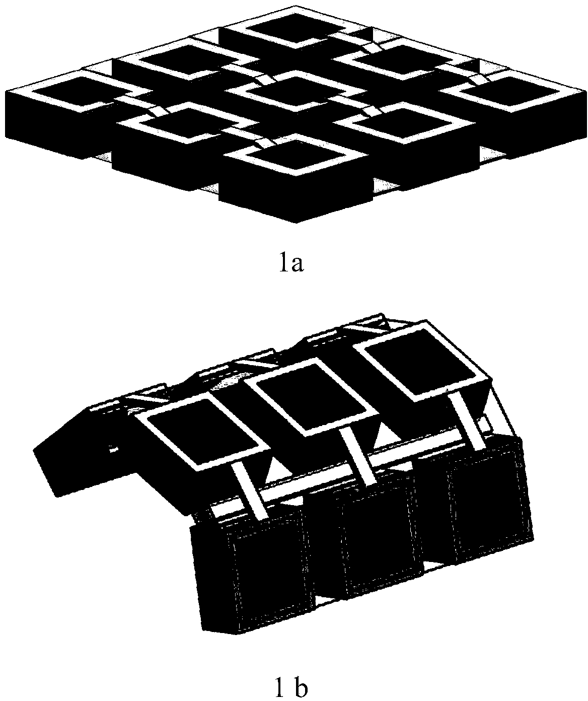
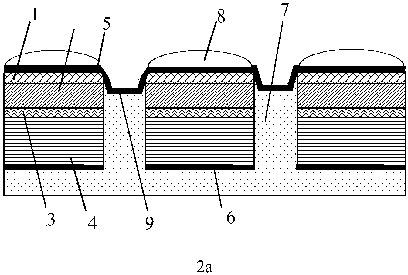
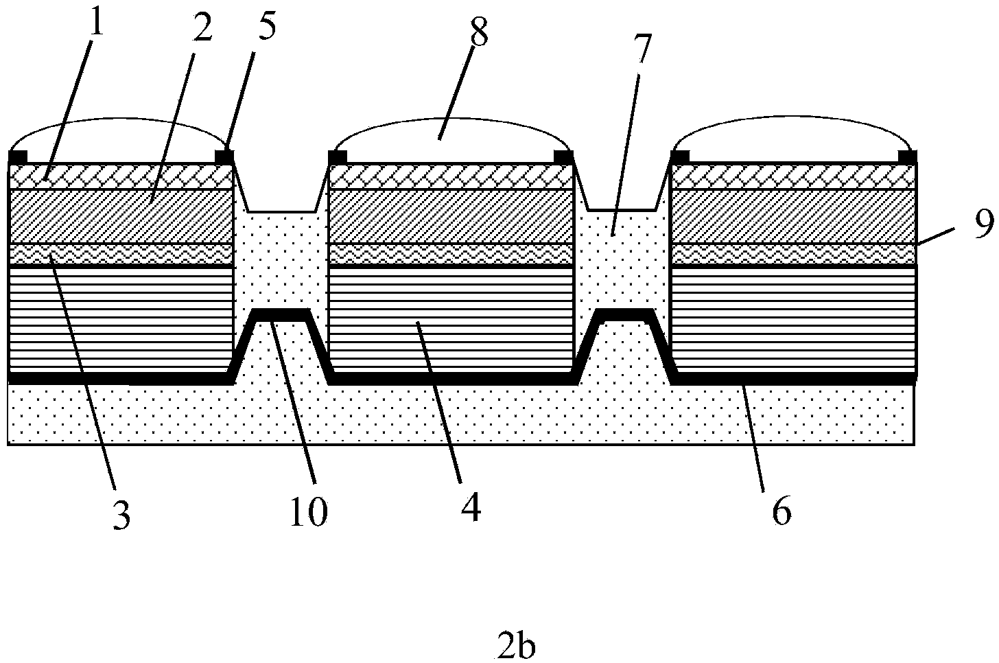
[0036] Specific implementation mode 1. Combination Figure 1 to Figure 8 Describe this embodiment mode, the flexible LED array device for microdisplay and lighting described in this embodiment mode, including: a light-transmitting layer 1, a light-emitting layer 2, a reflective layer 3, a substrate 4, an upper electrode 5, and an upper electrode lead 9 , the lower electrode 6, the lower electrode lead 10, the flexible area 7 and the microlens 8. The upper surface of the reflective layer 3 is the luminous layer 2 , the light-transmissive layer 1 and the microlens 8 in sequence, and the lower surface of the reflective layer 3 is the substrate 4 . The light-transmitting layer 1, the light-emitting layer 2, the reflective layer 3, the substrate 4 and the micro-lens 8 form an LED light-emitting unit. The LED light-emitting units are uniformly arranged to form a light-emitting unit array. There is a flexible area 7 between the light emitting units, and the flexible area 7 connects...

specific Embodiment approach 2

[0039] Specific embodiment two, combine Figure 9 and Figure 11 Describe this embodiment mode, this embodiment mode is the manufacturing method of the flexible LED array device for micro-display and lighting described in the first specific embodiment mode, this embodiment mode adopts the top-down manufacturing method, that is, the front structure is fabricated first, Then, protect the front structure and prepare the back structure. During the fabrication process, flexible electrodes are fabricated by filling flexible materials and photoetching special topography.

[0040] The basic process steps for preparing the flexible LED array device for micro-display and lighting according to the present invention are as follows:

[0041] A. Cleaning and front protection of light-emitting chips:

[0042] a) The host material used in the present invention is a light-emitting chip, and the light-emitting chip used is composed of a light-transmitting layer, a light-emitting layer, a ref...

specific Embodiment approach 3

[0064] Specific Embodiment 3. This embodiment is an embodiment of the method for preparing a flexible LED array device for micro-display and lighting described in Specific Embodiment 2: the specific process is as follows:

[0065] 1. Cleaning and front protection of light-emitting chips:

[0066] a) The light-emitting chip used in the present invention is an AlGaInP-LED epitaxial wafer, which is composed of a light-transmitting layer, a light-emitting layer, a reflective layer and a substrate, and the thickness of the light-emitting chip is 200 μm to 1000 μm.

[0067] b) The material of the upper protective film is silicon dioxide or silicon nitride or a composite film composed of silicon dioxide and silicon nitride or metal or organic material or inorganic material or other film materials that can play a protective role. The preparation method of the protective film is electron beam evaporation, radio frequency sputtering, magnetron sputtering, sol-gel method or other film gr...


PUM

PropertyMeasurementUnit
Depthaaaaaaaaaa
Thicknessaaaaaaaaaa
Thicknessaaaaaaaaaa

Abstract

The invention discloses a flexible LED array device for micro-displaying and lighting and a manufacture method, relates to the technical field of luminescence display, and solves the problem that a conventional plane surface type LED micro display piece is restricted when in use due to inflexibility. The operation processes of the flexibly connected LED device are that current is injected from upper electrodes and outflows from lower electrodes, an electric field is formed in the device, the positive and negative current carriers carry out recombination luminescence on luminous layers, part light passes through photic layers upwards, and is outshot from micro lens, and part light reach reflective layers downwards, is reflected by the reflective layers, penetrates through the luminous layers and the photic layers, and is outshot from the micro lens. As the luminous principle of the luminous device is the current carrier compound luminescence in p-n junction, the nonlinear characteristic of current voltage of a diode is provided; the luminous brightness is provided with the nonlinear characteristic along with the intensity of the injection current. Through the control of the brightness and the darkness of a pixel element by the circuit, the luminous display is realized.

Description

technical field [0001] The invention belongs to the technical field of luminescence display, and relates to a novel miniature flexible light emitting device, in particular to an AlGaInP-LED flexible micro device. Background technique [0002] In recent years, with the development of the electronic industry, micro light emitting devices have developed rapidly. Compared with traditional light-emitting devices, planar LED microdisplay arrays have many incomparable advantages, but because they cannot be bent, their application range is largely limited. Although OLED technology has good application prospects, compared with LED, there are still some shortcomings. For example, there are still some problems in micro-miniature devices, such as luminous brightness, uniformity, and luminous efficiency. Lifespan issues, these issues will limit the application and development of OLED to a large extent. With the development of science and technology, there is an increasingly urgent dema...

Claims


Application Information

Patent Timeline
IPC IPC(8): H01L27/15H01L33/00
Inventor 梁静秋王维彪梁中翥田超秦余欣吕金光高丹
Owner CHANGCHUN INST OF OPTICS FINE MECHANICS & PHYSICS CHINESE ACAD OF SCI
Why Eureka
Try Eureka