Method for manufacturing bifacial solar cell

A manufacturing method and solar cell technology, applied in the field of solar cells, can solve the problems of solar cell performance degradation, phosphorus diffusion and boron diffusion surface corrosion, high manufacturing costs, etc., to avoid pollution, high surface recombination rate, and photogenerated carrier recombination The effect of less and low manufacturing cost

Inactive Publication Date: 2013-12-25
SUZHOU RUNYANG PHOTOVOLTAIC TECH
View PDF5 Cites 10 Cited by
  • Summary
  • Abstract
  • Description
  • Claims
  • Application Information

AI Technical Summary

Problems solved by technology

However, this technical solution has the following disadvantages: first, the use of the mask layer increases two steps of mask layer deposition (step three) and mask layer removal (step six), and the manufacturing cost is relatively high; secondly, the mask layer may Existing harmful impurities and pollution introduced during the deposition of the mask layer may enter the interior of the solar cell during the subsequent phosphorus diffusion (step 5), thereby reducing the performance of the solar cell; finally, the high temperature of the phosphorus diffusion process often makes the mask The film layer becomes dense. In the subsequent mask layer removal step (step 6), the mask layer is difficult to remove. If the mask layer is removed by prolonging the process time or increasing the concentration of the etching solution, it will easily lead to phosphorus diffusion. and boron diffusion surface is corroded
However, the technical solution described in Document 3 has the following disadvantages: p-type ion implantation usually uses boron ions as the ion source, but boron implantation will form lattice damage such as high-density point defects on the surface of the semiconductor substrate. The heat treatment is still difficult to be completely eliminated
This part of the point defect will become the center of the recombination of photogenerated carriers in the solar cell, resulting in a decrease in the performance of the solar cell.
In addition, in addition to boron ion implantation, other p-type impurity ion implantation techniques have not been fully studied in the field of solar cell fabrication

Method used


Image

  • Method for manufacturing bifacial solar cell
  • Method for manufacturing bifacial solar cell
  • Method for manufacturing bifacial solar cell

Examples


Embodiment 1

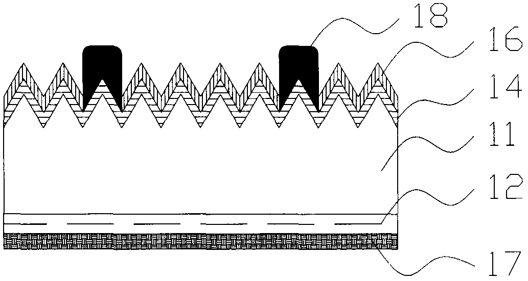
[0065] Embodiment 1 of the present invention discloses a method for manufacturing a double-sided light-receiving solar cell. The flow chart and the schematic diagram of the solar cell structure corresponding to each step are as follows Figure 4 ~ Figure 11 As shown, it specifically includes the following steps:

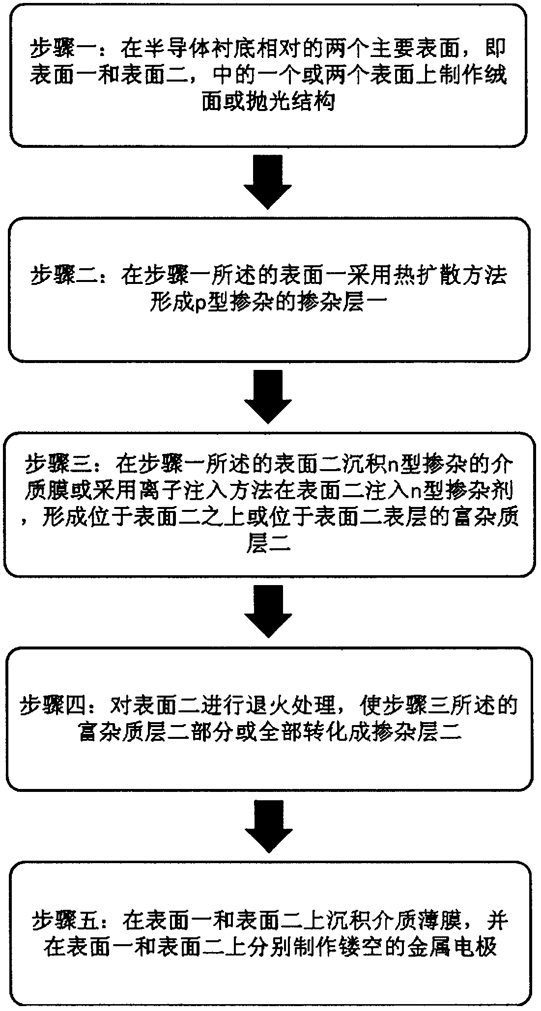
[0066] Step 1: If Figure 4 and Figure 5 As shown, a textured structure is fabricated on the two opposite main surfaces of a semiconductor substrate 21, such as a crystalline silicon wafer, namely surface one 21a and surface two 21b. The above steps are carried out by wet chemical etching, and the thickness of the material removed from the surface layer of the semiconductor substrate is between 3-8 um, for example 5 um.

[0067] Step 2: If Figure 6 As shown, a p-type doped doped layer 22 is formed on the surface 1 21a in step 1 by thermal diffusion. In the above steps, the textured semiconductor substrate 21 is placed in an environment filled with boron tribrom...

Embodiment 2

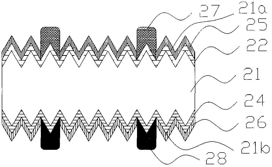
[0073] Embodiment 2 of the present invention discloses a method for manufacturing a double-sided light-receiving solar cell. The flow chart and the schematic diagram of the solar cell structure corresponding to each step are as follows: Figure 12 to Figure 19 As shown, it specifically includes the following steps:

[0074] Step 1: If Figure 12 and Figure 13 As shown, a textured structure is fabricated on the two opposite main surfaces of a semiconductor substrate 31, such as a crystalline silicon wafer, namely surface one 31a and surface two 31b. The above steps are carried out by wet chemical etching, and the thickness of the material removed from the surface layer of the semiconductor substrate is between 3-8 um, for example 5 um.

[0075] Step 2: If Figure 14 As shown, a p-type doped doped layer 32 is formed on the surface 1 31a in step 1 by thermal diffusion. In the above steps, the textured semiconductor substrate 31 is placed in an environment filled with boron t...


PUM

PropertyMeasurementUnit
thicknessaaaaaaaaaa
thicknessaaaaaaaaaa

Abstract

The invention belongs to the field of solar cells, and proposes a method for manufacturing a solar cell. Specifically, the method for manufacturing a solar cell comprises a step of manufacturing textured surface or polished structures on two main surfaces of a substrate; a step of forming a p-type doped doping layer One on a main surface One of the substrate through thermal diffusion; a step of depositing an n-type doped medium membrane on the main surface Two of the substrate or injecting n-type dopant in the main surface Two of the substrate by using an ion injection method; a step of performing annealing processing on the main surface Two of the substrate to form an n-type doped doping layer Two; and a step of depositing medium thin films and hollow-out metal electrodes on the two main surfaces of the substrate. The method is mainly used for manufacturing bifacial solar cells. Compared with methods in the prior art, the method solves technical problems that the manufacture of the bifacial solar cell requires that mutually isolated doping layers be formed on the two main surfaces of the semiconductor substrate in a simpler way, helps to reduce the manufacturing cost and meanwhile helps to improve device performance.

Description

technical field [0001] The invention relates to a manufacturing method of a double-sided light-receiving solar cell, which belongs to the field of solar cells. Background technique [0002] A solar cell is a semiconductor optoelectronic device that uses the photovoltaic effect to convert sunlight into usable electrical energy. Receiving as much sunlight as possible and reducing the recombination of photogenerated carriers as much as possible are the two main ways to increase the actual power generation of solar cells. The structure of traditional structure solar cells is as follows figure 1 shown. Its main structure includes: a semiconductor substrate (11), generally crystalline silicon; a doped layer (14) located on one of the main surfaces of the semiconductor substrate; a dielectric film (16) covering the doped layer; The hollow metal electrode (18) on the part of the layer is generally a silver electrode; the metal electrode (17) covering most of the other main surfac...

Claims


Application Information

Patent Timeline
Patent Type & Authority Applications(China)
IPC IPC(8): H01L31/18
CPCY02P70/50
Inventor 杨灼坚陶龙忠
Owner SUZHOU RUNYANG PHOTOVOLTAIC TECH
Why Eureka
Try Eureka