High-sensitivity terahertz microfluidic channel sensor and preparation method thereof
一种微流通道、太赫兹的技术,应用在传感器领域,能够解决灵敏度有限、受限消逝波重叠程度等问题,达到高灵敏检测的效果
- Summary
- Abstract
- Description
- Claims
- Application Information
AI Technical Summary
Problems solved by technology
Method used
Image
Examples
Embodiment 1
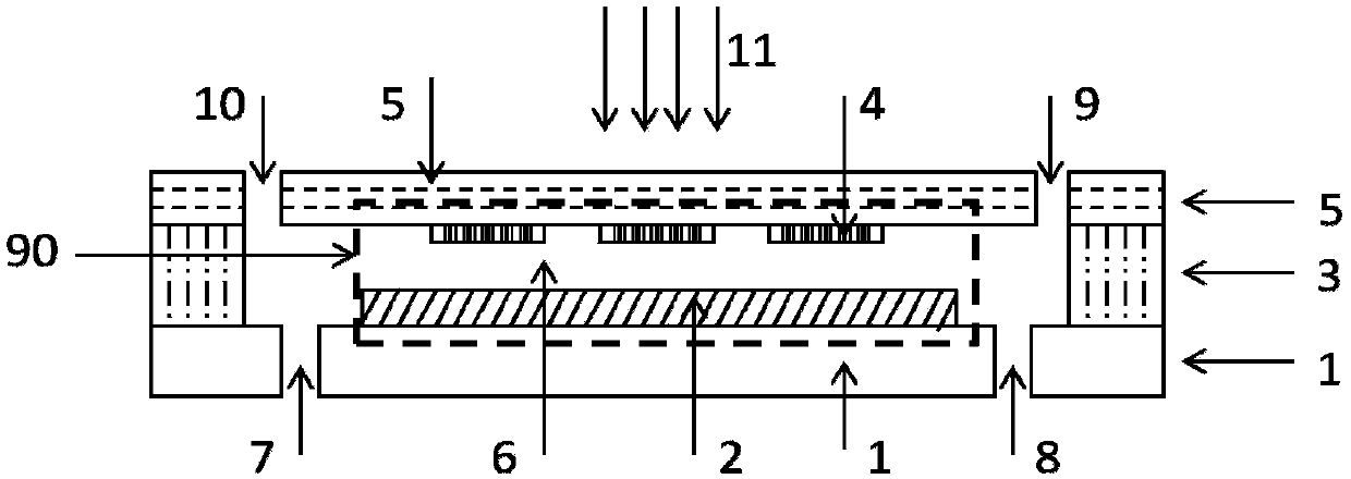
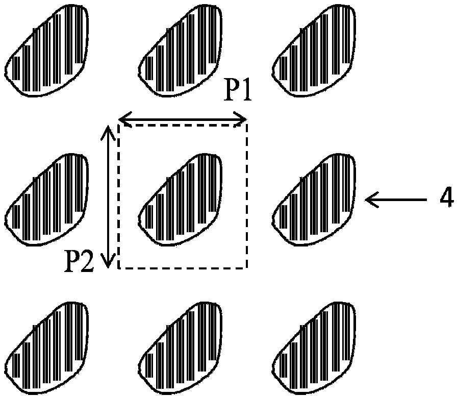
[0063] In this example, with figure 1 , image 3 The structure diagram shown and Figure 5 The process flow diagram shown is taken as an example for illustration. The preparation process of the high-sensitivity terahertz microfluidic channel sensor includes: firstly, the metal plane mirror 2 is prepared on the substrate 1 by depositing a metal thin film ( Figure 5 (a)); secondly, on the cover layer 5, the metal microstructure layer 4 is prepared by micro-nano processing methods such as photolithography, thin film deposition and lift-off technology ( Figure 5 (b)), then, on the substrate 1 and the cover layer 5, the bonding material layer 3 is prepared by a micro-nano processing method ( Figure 5 (c)); The substrate 1 is connected with the cover layer 5 by an interlayer bonding method, and a closed microfluidic channel 6 is formed in the middle ( Figure 5 (d)); Finally, form the input and output ports 7, 8, 9 and 10 on the substrate 1 or the cover layer 5 by etching or ...
Embodiment 2
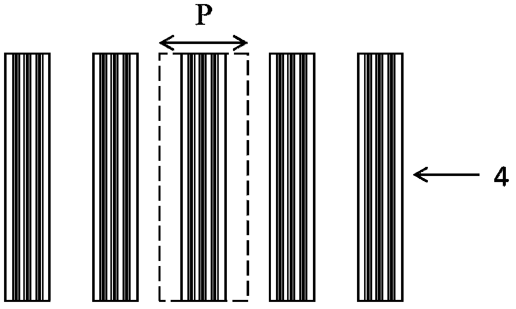
[0068] The structure and process in this embodiment are the same as in Embodiment 1. As another optimized structural parameter, the metal microstructure layer 4 is a cross structure with a period of 56 microns, an arm length of 40 microns, and an arm width of 4 microns. The height of the fluid channel 6 is 4 microns. Depend on Figure 13 and Figure 14 The relationship between the frequency of the resonant absorption peak and the absorptivity with the change of the refractive index of the liquid in the fluid channel 6, it can be seen that the resonance causes a strong absorption, and when the refractive index of the liquid in the fluid channel 6 changes, the frequency of the resonant absorption peak and the absorption rate change. The sensitivity of the terahertz microfluidic channel sensor designed in the present invention is 0.98THz / RIU, which is 2.5 times of the sensor (sensitivity 0.38THz / RIU) that the microfluidic channel is integrated on the surface of the metal micros...
Embodiment 3
[0070] refer to Figure 6 Shown is a schematic diagram of a longitudinal section of a high-sensitivity terahertz microfluidic channel sensor in this embodiment. The difference from the first embodiment is that the surface of the metal plane mirror 2 and the metal microstructure layer 4 contains a layer of dielectric protection layer 12, such as two Silicon oxide, silicon nitride, aluminum oxide and SU-8 photoresist, etc., the thickness of which is 10-100 nanometers. The dielectric protection layer 12 introduced in this structure can better improve the stability of the terahertz microfluidic channel sensor.
PUM
| Property | Measurement | Unit |
|---|---|---|
| refractive index | aaaaa | aaaaa |
Abstract
Description
Claims
Application Information


