Wet process chemical preparation method for black silicon with pointed-cone-shaped surface

A wet chemistry, black silicon technology, applied in final product manufacturing, sustainable manufacturing/processing, semiconductor/solid-state device manufacturing, etc., can solve the problem of uneven distribution of nanowire structures, actual production cost requirements, low current collection efficiency, etc. problem, to achieve the effect of good repeated use, controllable morphology, and small residual stress

Active Publication Date: 2014-02-12
ZHEJIANG UNIV OF TECH
View PDF3 Cites 19 Cited by
  • Summary
  • Abstract
  • Description
  • Claims
  • Application Information

AI Technical Summary

Problems solved by technology

At present, most researchers mainly focus on noble metal-assisted etching methods (Ag, Pt, Au, etc.), and the research results have tended to be finalized. Considering the uneven distribution of nanow

Method used


Image

  • Wet process chemical preparation method for black silicon with pointed-cone-shaped surface
  • Wet process chemical preparation method for black silicon with pointed-cone-shaped surface
  • Wet process chemical preparation method for black silicon with pointed-cone-shaped surface

Examples


Embodiment 1

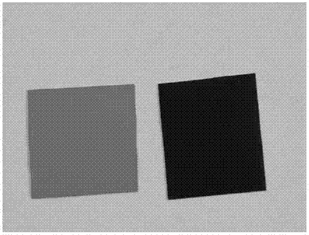
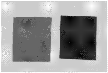
[0037](1) Prepare the first etching solution, that is, 100 mL of a mixed solution of copper nitrate, hydrofluoric acid and hydrogen peroxide, in which the concentration of copper nitrate is 46.5 mmol / L, the volume fraction of hydrofluoric acid is 8%, and the peroxide The volume fraction of hydrogen is 38%, and the solvent is deionized water. Put the monocrystalline silicon sample after the RCA cleaning process into the first etching solution at 55°C, take out the silicon wafer after 60 minutes, wash the surface with a large amount of deionized water, and dry it to obtain the initially etched monocrystalline silicon sample . After characterization tests, it can be obtained as image 3 In the top view of the SEM shown, due to a layer of residue on the surface, the macroscopic appearance is brownish yellow.

[0038] (2) Prepare the second etching solution, that is, 50 mL of a mixed solution of copper nitrate, hydrogen peroxide and ammonium bifluoride, in which the concentration...

Embodiment 2

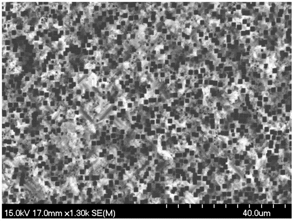
[0040] (1) Prepare the first etching solution, that is, 100 mL of a mixed solution of copper nitrate, hydrofluoric acid and hydrogen peroxide, in which the concentration of copper nitrate is 49.6 mmol / L, the volume fraction of hydrofluoric acid is 10%, and the peroxide The volume fraction of hydrogen is 36%, and the solvent is deionized water. Put the single crystal silicon sample after the RCA cleaning process into the first etching solution at 50°C, take out the silicon wafer after 50 minutes, wash the surface with a large amount of deionized water, and dry it to obtain the initial etched single crystal silicon sample . After characterization tests, it can be obtained as Figure 4 In the top view of the SEM shown, since there is also a layer of residue on the surface, the macroscopic appearance is brownish yellow; the surface of the black silicon forms a relatively uniform tetragonal porous layer with a pore size of about 2um.

[0041] (2) Prepare the second etching soluti...

Embodiment 3

[0043] (1) Prepare the first etching solution, that is, 100 mL of a mixed solution of copper nitrate, hydrofluoric acid and hydrogen peroxide, in which the concentration of copper nitrate is 51.2 mmol / L, the volume fraction of hydrofluoric acid is 8%, and the peroxide The volume fraction of hydrogen is 36%, and the solvent is deionized water. Put the monocrystalline silicon sample after the RCA cleaning process into the first etching solution at 45°C, take out the silicon wafer after 50 minutes, wash the surface with a large amount of deionized water, and dry it to obtain the initially etched monocrystalline silicon sample . There is also a layer of residue on the surface, which is brownish-yellow macroscopically.

[0044] (2) Prepare the second etching solution, that is, 50 mL of a mixed solution of copper nitrate, hydrogen peroxide and ammonium bifluoride, in which the concentration of copper nitrate is 28.4 mmol / L, the volume fraction of hydrogen peroxide is 28%, and the c...


PUM

PropertyMeasurementUnit
Concentrationaaaaaaaaaa
Apertureaaaaaaaaaa
Volume fractionaaaaaaaaaa

Abstract

The invention discloses a wet process chemical preparation method for black silicon with a pointed-cone-shaped surface. The preparation method comprises the steps that two kinds of etching liquid are prepared, wherein the first kind of etching liquid is mixing water solution of nitric acid copper, hydrogen peroxide and hydrofluoric acid, and the second kind of etching liquid is mixing water solution of nitric acid copper, ammonium hydrogen fluoride and hydrogen peroxide; a monocrystalline silicon piece is placed into the first kind of etching liquid for initial etching; the monocrystalline silicon piece is placed into the second kind of etching liquid for surface structural ornament; finally, surface metal granule residue is washed, and the black silicon materials with the pointed-cone-shaped surface are obtained. According to the preparation method, two steps of copper ion chemical auxiliary etching is utilized, and a pointed-cone-shaped nanometer structure is prepared on the surface of monocrystalline silicon. The structure has good light trapping performance, and can remarkably improve light absorbing efficiency when applied to a silicon substrate solar cell.

Description

(1) Technical field [0001] The invention relates to a wet chemical preparation method of black silicon with a tapered surface, in particular to a black silicon material with a tapered micro-nano structure on the surface that is assisted by two-step chemical catalysis of metal copper ions on single crystal silicon. , which belongs to the field of micromachining of semiconductor materials. (2) Background technology [0002] As the world works together to pay attention to "sustainable development and low-carbon society", renewable energy technology, especially photovoltaic solar energy industry, is facing enormous development challenges. At the same time, how to effectively improve the photoelectric conversion efficiency of solar cells has become a research hotspot among scholars all over the world. With the rise of the photovoltaic industry and the in-depth research on solar cell surface engineering, the preparation of black silicon materials with micro-nano structures on the...

Claims


Application Information

Patent Timeline
IPC IPC(8): H01L21/306H01L31/18
CPCH01L21/30604H01L31/1804Y02E10/547Y02P70/50
Inventor 丁月卢建树
Owner ZHEJIANG UNIV OF TECH
Why Eureka
Try Eureka