Polycrystalline silicon/monocrystalline silicon heterojunction structure applied to solar cell and preparation method thereof
A technology of solar cells and polysilicon, applied in circuits, photovoltaic power generation, electrical components, etc., can solve problems such as unfavorable mastery, high process requirements, failure to break the monopoly position of solar cells, etc., to reduce storage time, wide selection range, save energy effect
- Summary
- Abstract
- Description
- Claims
- Application Information
AI Technical Summary
Problems solved by technology
Method used
Image
Examples
Embodiment 1
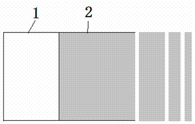
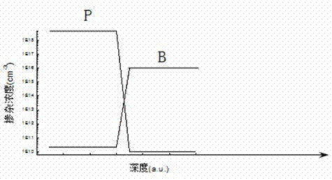
[0021] A uniformly doped polysilicon thin film / single crystal silicon heterojunction structure for solar cells such as figure 1 As shown, the distribution of doping elements phosphorus (P) and boron (B) is as follows figure 2 As shown, the p-type silicon wafer is used as an example for illustration here, but the silicon wafer is not limited to this, n-type silicon wafers can also be used, but the emitter doping type, process method, etc. need to be adjusted. Necessary illustrations are carried out to the structure and its preparation method below:
[0022] 1) For the uniformly doped polysilicon thin film 1 of the emitter, the doping concentration of this layer is 2×10 18 cm -3 , the thickness can be adjusted between 10 and 500 nm, and 100 nm is selected here.
[0023] 2) The preparation method of this layer can adopt the following process flow, but not limited thereto. First, one side of the monocrystalline silicon wafer 2 that needs to be deposited is cleaned as necessa...
Embodiment 2
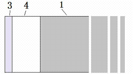
[0025] A polysilicon thin film / single crystal silicon heterojunction structure with double layers of different doping concentrations for solar cells such as image 3 As shown, the distribution of doping elements phosphorus (P) and boron (B) is as follows Figure 4 shown. Here, the p-type silicon wafer is taken as an example for illustration, but the silicon wafer is not limited to this, n-type silicon wafers can also be used, but the emitter doping type, process method, etc. need to be adjusted. Necessary illustrations are carried out to the structure and its preparation method below:
[0026] 1) The doping concentration of the polysilicon thin film 3 with high doping concentration is 2×10 19 cm -3 , and the thickness can vary between 3 and 50 nm, which is selected as 10 nm here; the doping concentration of the polysilicon thin film 4 with low doping concentration is 1×10 18 cm -3 , the thickness can vary from 20 to 500 nm, here is selected as 100 nm;
[0027] 2) The pr...
Embodiment 3
[0029] A patterned high-doped polysilicon thin film / low-doped polysilicon thin film / monocrystalline silicon heterojunction structure for solar cells such as Figure 5 As shown, the distribution of doping elements phosphorus (P) and boron (B) is as follows Figure 6 shown. Here, the p-type silicon wafer is taken as an example for illustration, but the silicon wafer is not limited to this, n-type silicon wafers can also be used, but the emitter doping type, process method, etc. need to be adjusted. Necessary illustrations are carried out to the structure and its preparation method below:
[0030] 1) The doping concentration of the patterned polysilicon film 5 with high doping concentration is 2×10 19 cm -3 , and the thickness can vary between 3 and 50 nm, which is selected as 10 nm here; the doping concentration of the polysilicon thin film 4 with low doping concentration is 1×10 18 cm -3 , the thickness can vary from 20 to 500 nm, here is selected as 100 nm;
[0031] Th...
PUM
| Property | Measurement | Unit |
|---|---|---|
| Thickness | aaaaa | aaaaa |
| Doping concentration | aaaaa | aaaaa |
| Thickness | aaaaa | aaaaa |
Abstract
Description
Claims
Application Information
 - R&D Engineer
- R&D Manager
- IP Professional
- Industry Leading Data Capabilities
- Powerful AI technology
- Patent DNA Extraction
Browse by: Latest US Patents, China's latest patents, Technical Efficacy Thesaurus, Application Domain, Technology Topic, Popular Technical Reports.
© 2024 PatSnap. All rights reserved.Legal|Privacy policy|Modern Slavery Act Transparency Statement|Sitemap|About US| Contact US: help@patsnap.com


