Electret-structure-introduced efficient solar cell and preparing method thereof

A technology of solar cells and electrets, applied in circuits, photovoltaic power generation, electrical components, etc., can solve the problems of poor stability, low fixed charge density of thin films, weak field passivation, etc., to improve open circuit voltage, reduce compounding, Reduce the effect of efficiency decay

Active Publication Date: 2014-03-26
ZHONGWEI NEW ENERGY CHENGDU CO LTD
View PDF3 Cites 13 Cited by
  • Summary
  • Abstract
  • Description
  • Claims
  • Application Information

AI Technical Summary

Problems solved by technology

These surface passivation films deposited by conventional methods have very low fixed charge density and poor stability, mainly due to the surface chemical passivation of the film, and the field passivation effect is very weak.
[0018] Although electret has been studied a lot in the field of integrated circuits, it has been a very mature technology, but there are few reports in the field of solar cells, so the present invention attempts to introduce a thin layer of electret in the structure of conventional solar cells. Bulk materials for field passivation of solar cells

Method used


Image

  • Electret-structure-introduced efficient solar cell and preparing method thereof
  • Electret-structure-introduced efficient solar cell and preparing method thereof
  • Electret-structure-introduced efficient solar cell and preparing method thereof

Examples


Embodiment 1

[0035] Embodiment 1: the preparation steps of monolayer film corona charging electretization are:

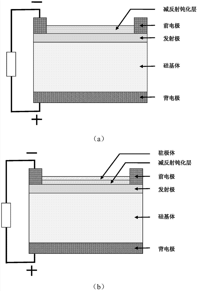
[0036] 1. After the p-type silicon wafer with a thickness of 280±10 microns and a resistivity of 3 ohm cm is cleaned and textured, it is doped with phosphorus in a high-temperature diffusion furnace to form a p-N junction. Diffusion forms an N-type surface with a sheet resistance of 60 ohms / □. Plasma edge etching, cleaning away the surface phosphosilicate glass.

[0037] 2. A silicon nitride film with a refractive index of 2.05 and a thickness of 80 nanometers is grown on the N-type surface by PECVD.

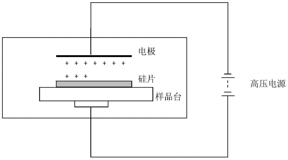
[0038] 3. Perform electret treatment on the silicon nitride film. Corona charging is performed on the silicon nitride surface of the silicon wafer. The charging voltage is 6 kV, the electrode is 2 cm away from the surface of the silicon wafer, and the charging time is 80 seconds.

[0039] 4. Perform annealing treatment on the surface-treated silicon wafer at 380 degrees Celsiu...

Embodiment 2

[0042]Embodiment 2: the method step of the anti-reflection passivation film of direct deposition electret structure is:

[0043] 1. After the p-type silicon wafer with a thickness of 280±10 microns and a resistivity of 3 ohm cm is cleaned and textured, it is doped with phosphorus in a high-temperature diffusion furnace to form a p-N junction. Diffusion forms an N-type surface with a sheet resistance of 60 ohms / □. Plasma edge etching, cleaning away the surface phosphosilicate glass.

[0044] 2. On the N-type surface, a silicon nitride electret thin film with a refractive index of 2.05 and a thickness of 80 nanometers is deposited by an electret-optimized plasma vapor deposition method.

[0045] 3. Perform annealing treatment at 380 degrees Celsius for 60 seconds on the silicon wafer on which the silicon nitride electret film is grown.

[0046] 4. Print the back electrode, the back field and the front electrode, sinter and test.

[0047] In this embodiment, an anti-reflection...

Embodiment 3

[0048] Embodiment 3: the preparation step of ion implantation electretization to monolayer membrane comprises:

[0049] 1. After the p-type silicon wafer with a thickness of 280±10 microns and a resistivity of 3 ohm cm is cleaned and textured, it is doped with phosphorus in a high-temperature diffusion furnace to form a p-N junction. Diffusion forms an N-type surface with a sheet resistance of 60 ohms / □. Plasma edge etching, cleaning away the surface phosphosilicate glass.

[0050] 2. A silicon nitride film with a refractive index of 2.05 and a thickness of 80 nanometers is grown on the N-type surface by PECVD.

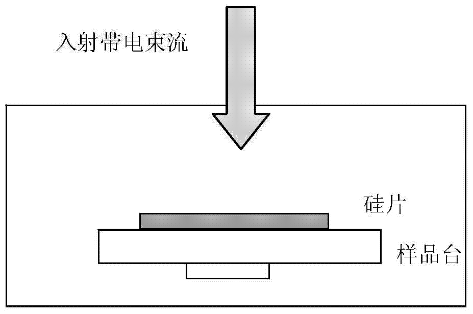
[0051] 3. Perform electret treatment on the silicon nitride film. Ion implantation is performed on the silicon nitride film on the surface of the silicon wafer. The implanted ion source is helium particles, the voltage is 3 kV, and the implantation dose is: 10 13 / cm 2 .

[0052] 4. Perform annealing treatment on the surface-treated silicon wafer at 350 degrees ...


PUM


Abstract

The invention relates to an electret-structure-introduced efficient solar cell and a preparing method thereof. The electret-structure-introduced efficient solar cell and the preparing method thereof are characterized in that an electret thin layer is introduced into a traditional solar cell structure to improve the monochromatic incident photon-to-electron conversion efficiency of the solar cell. The introduced electret structure can be obtained through any one of the four modes of 1) performing electret treatment on a surface passivation antireflection film of the solar cell to enable the solar cell to have an electret function; 2) or separately depositing an electret thin layer on the surface of the solar cell; 3) or introducing encapsulating materials with electret properties into component encapsulation; 4) or inducing an electret thin layer in a cell or a component through treatment of electret means after the preparation of the solar cell or the component is completed. The electret-structure-introduced efficient solar cell and the preparing method thereof are not only applicable to crystalline silicon cells, but also applicable to solar cells of other types such as amorphous silicon thin film cells, cadmium telluride cells, gallium arsenide cells, copper indium gallium diselenide cells, dye-sensitized cells and organic cells.

Description

technical field [0001] The invention relates to a solar cell with an electret structure and a preparation method thereof, belonging to the field of new energy. Background technique [0002] Nowadays, due to the continuous shortage of petrochemical energy that supports the development of human civilization, and the increasing demand for energy, how to provide green and renewable energy to support the sustainable development of mankind has become the most urgent problem. Among various alternative energy sources, solar photovoltaic power generation is the most advantageous. The photovoltaic market has grown at a rate of more than 40% in recent years. In 2011, the output of photovoltaic modules exceeded 26 GW, and the output value exceeded 300 billion. Solar cells are the core part of solar photovoltaic power generation system. [0003] With the continuous improvement of commercial solar battery conversion efficiency. The recombination of photogenerated carriers has become th...

Claims


Application Information

Patent Timeline
Patent Type & Authority Applications(China)
IPC IPC(8): H01L31/0216H01L31/068H01L31/18
CPCY02E10/50H01L31/02168H01L31/0481H01L31/186Y02E10/542Y02E10/547Y02P70/50
Inventor 刘金宁刘正新孟凡英
Owner ZHONGWEI NEW ENERGY CHENGDU CO LTD
Why Eureka
Try Eureka