A high-efficiency solar cell with electret structure and its preparation method
A technology of solar cells and electrets, applied in circuits, photovoltaic power generation, electrical components, etc., can solve the problems of poor stability, low fixed charge density of thin films, weak field passivation, etc., to improve open circuit voltage, reduce compounding, Reduce the effect of efficiency decay
- Summary
- Abstract
- Description
- Claims
- Application Information
AI Technical Summary
Problems solved by technology
Method used
Image
Examples
Embodiment 1
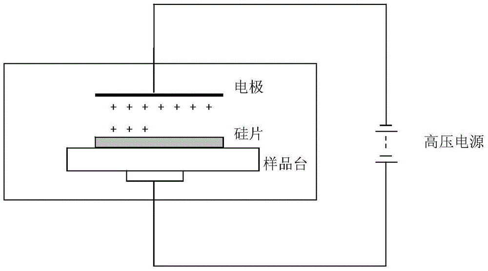
[0035] Embodiment 1: the preparation steps of monolayer film corona charging electretization are:
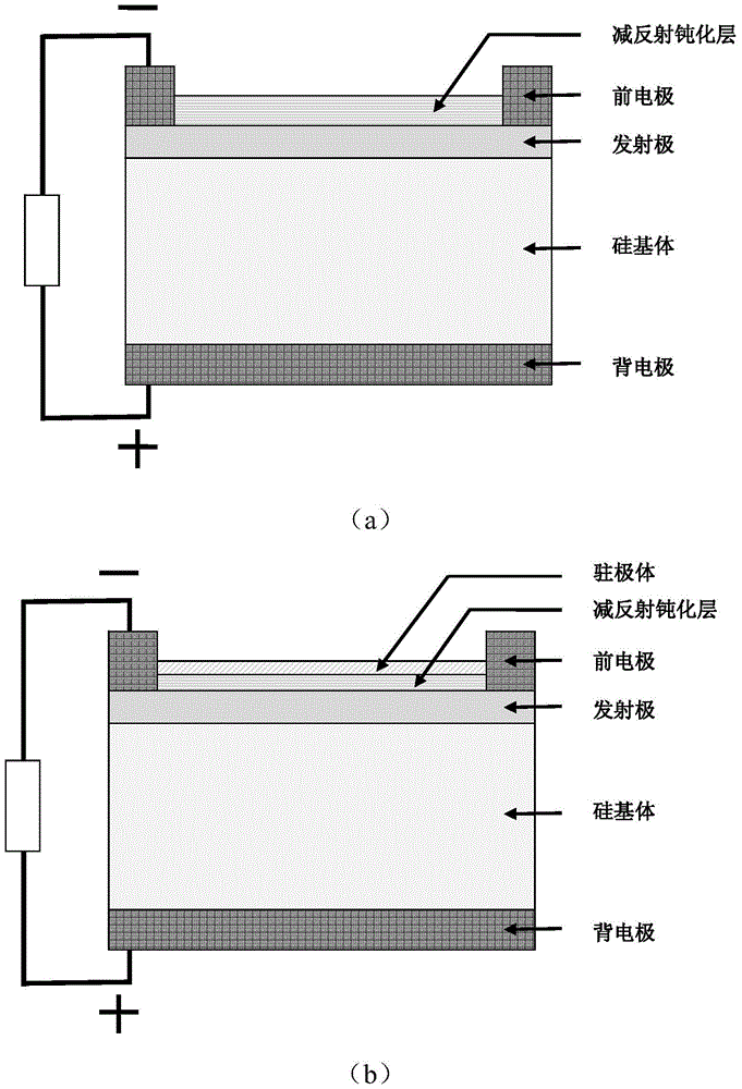
[0036] 1. After the p-type silicon wafer with a thickness of 280±10 microns and a resistivity of 3 ohm cm is cleaned and textured, it is doped with phosphorus in a high-temperature diffusion furnace to form a p-N junction. Diffusion forms an N-type surface with a sheet resistance of 60 ohms / □. Plasma edge etching, cleaning away the surface phosphosilicate glass.
[0037] 2. A silicon nitride film with a refractive index of 2.05 and a thickness of 80 nanometers is grown on the N-type surface by PECVD.
[0038] 3. Perform electret treatment on the silicon nitride film. Corona charging is carried out on the silicon nitride surface of the silicon wafer. The charging voltage is 6 kV, the electrode is 2 cm away from the surface of the silicon wafer, and the charging time is 80 seconds.
[0039] 4. Perform annealing treatment on the surface-treated silicon wafer at 380 degrees Cels...
Embodiment 2
[0042] Embodiment 2: the method step of the anti-reflection passivation film of direct deposition electret structure is:
[0043]1. After the p-type silicon wafer with a thickness of 280±10 microns and a resistivity of 3 ohm cm is cleaned and textured, it is doped with phosphorus in a high-temperature diffusion furnace to form a p-N junction. Diffusion forms an N-type surface with a sheet resistance of 60 ohms / □. Plasma edge etching, cleaning away the surface phosphosilicate glass.
[0044] 2. On the N-type surface, a silicon nitride electret thin film with a refractive index of 2.05 and a thickness of 80 nanometers is deposited by an electret-optimized plasma vapor deposition method.
[0045] 3. Perform annealing treatment at 380 degrees Celsius for 60 seconds on the silicon wafer on which the silicon nitride electret film is grown.
[0046] 4. Print the back electrode, the back field and the front electrode, sinter and test.
[0047] In this embodiment, an anti-reflection...
Embodiment 3
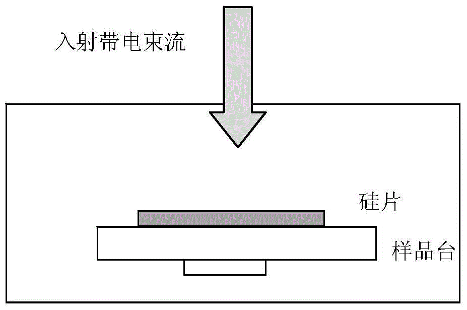
[0048] Embodiment 3: the preparation step of ion implantation electretization to monolayer membrane comprises:
[0049] 1. After the p-type silicon wafer with a thickness of 280±10 microns and a resistivity of 3 ohm cm is cleaned and textured, it is doped with phosphorus in a high-temperature diffusion furnace to form a p-N junction. Diffusion forms an N-type surface with a sheet resistance of 60 ohms / □. Plasma edge etching, cleaning away the surface phosphosilicate glass.
[0050] 2. A silicon nitride film with a refractive index of 2.05 and a thickness of 80 nanometers is grown on the N-type surface by PECVD.
[0051] 3. Perform electret treatment on the silicon nitride film. Ion implantation is performed on the silicon nitride film on the surface of the silicon wafer. The implanted ion source is helium particles, the voltage is 3 kV, and the implantation dose is: 10 13 / cm 2 .
[0052] 4. Perform annealing treatment on the surface-treated silicon wafer at 350 degrees ...
PUM
 Abstract
Description
Claims
Application Information


