Method for manufacturing black silicon materials

A black silicon and silicon substrate technology, applied in the field of photoelectric sensitive materials, can solve the problems of poor thermodynamic performance and crystal quality, limited application, high price, etc., and achieve a wide range of absorption wavelengths, huge application potential, and high absorption rate. Effect

Inactive Publication Date: 2014-03-26
UNIV OF ELECTRONIC SCI & TECH OF CHINA
View PDF9 Cites 8 Cited by
  • Summary
  • Abstract
  • Description
  • Claims
  • Application Information

AI Technical Summary

Problems solved by technology

However, these materials are relatively expensive, have poor thermodynamic properties and crystal quality, and are not compa

Method used


Image

  • Method for manufacturing black silicon materials

Examples


Embodiment Construction

[0021] The specific steps of the method for manufacturing black silicon material according to the embodiment of the present invention will be described in detail below with reference to the accompanying drawings.

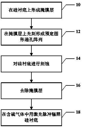
[0022] Such as figure 1 As shown, in the embodiment of the present invention, a method for manufacturing black silicon material includes step 10 , step 12 , step 14 , step 16 and step 18 . Each step will be described in detail below in conjunction with specific embodiments.

[0023] Step 10: forming a mask layer on the silicon substrate.

[0024] In an embodiment of the present invention, firstly a mask layer is formed on a silicon substrate.

[0025] In an embodiment of the present invention, the mask layer here may be a silicon nitride mask layer or a silicon oxide mask layer, and its thickness may be 90 to 600 nanometers. The silicon nitride mask layer or the silicon oxide mask layer can be formed on the silicon substrate by a deposition method, such as plasma...


PUM

PropertyMeasurementUnit
Wavelengthaaaaaaaaaa

Abstract

The embodiment of the invention discloses a method for manufacturing black silicon materials. The method comprises the steps that a mask layer is formed on a silicon substrate; a preset graph through hole array is formed in the mask layer in a photoetching mode; the silicon substrate is etched, and a preset graph groove array is formed in the silicon substrate; the mask layer is removed from the silicon substrate; the silicon substrate is put into sulfurous gas, laser pulse radiates the silicon substrate, and the black silicon materials are obtained. According to the method for manufacturing the black silicon materials, high-energy laser is used for radiating a periodic array structure on the silicon substrate in a sulfurous gas environment, so that a micro-nano dual structure is formed, and sulfur doping is achieved at the same time in the radiation process. The absorption wave length of the obtained black silicon materials is expanded, the absorption rate is higher, the range of the absorption wave length is larger, and process steps are simple.

Description

technical field [0001] The invention relates to the technical field of photoelectric sensitive materials, in particular to a method for manufacturing black silicon materials. Background technique [0002] Silicon material is an important semiconductor material. Because of its characteristics of easy purification, easy doping, and high temperature resistance, it has been widely used in many fields such as microelectronics, photovoltaic industry, and communication industry. However, due to the limitation of its forbidden band width, crystalline silicon materials cannot absorb light waves with wavelengths greater than 1100 nanometers (nm). When the incident light wavelength is greater than 1100nm, the absorption rate and responsivity of silicon-based detectors to light will be greatly reduced. Therefore, photodetector devices with operating wavelengths greater than 1100nm are generally made of materials such as germanium and gallium indium arsenide. However, these materials a...

Claims


Application Information

Patent Timeline
IPC IPC(8): H01L31/18H01L31/028H01L31/0288
CPCH01L21/268H01L31/1804Y02P70/50
Inventor 李世彬张婷吴志明蒋亚东
Owner UNIV OF ELECTRONIC SCI & TECH OF CHINA
Why Eureka
Try Eureka