Fabrication method of gallium nitride laser cavity surface

A manufacturing method and laser technology, applied to lasers, laser components, semiconductor lasers, etc., can solve the problems of increased laser threshold density, uneven bombardment, and inability to generate resonance, so as to improve reflectivity, simplify the process, and eliminate damage Effect

Active Publication Date: 2014-04-02
INST OF SEMICONDUCTORS - CHINESE ACAD OF SCI
View PDF4 Cites 12 Cited by
  • Summary
  • Abstract
  • Description
  • Claims
  • Application Information

AI Technical Summary

Problems solved by technology

[0004] Generally speaking, the gallium nitride laser grown on the sapphire substrate adopts the method of inductive plasma etching to formulate the cavity surface of the resonator required for laser resonance, but this manufacturing method will cause damage to the laser during the etching process. The uneven bombardment of the cavity surface leads to stripe-like damage on the surface. According to related literature, the stripe-like damage on the surfac...

Method used


Image

  • Fabrication method of gallium nitride laser cavity surface
  • Fabrication method of gallium nitride laser cavity surface
  • Fabrication method of gallium nitride laser cavity surface

Examples


Embodiment Construction

[0029] In order to make the object, technical solution and advantages of the present invention clearer, the present invention will be further described in detail below in conjunction with specific embodiments and with reference to the accompanying drawings.

[0030] The invention provides a method for manufacturing a cavity surface of a gallium nitride laser, comprising the following steps:

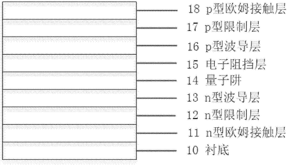
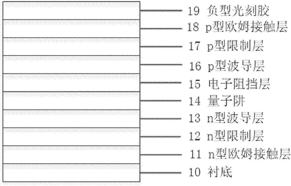
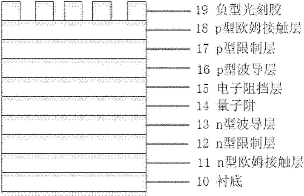
[0031] Step S1: epitaxially growing a gallium nitride laser structure on the substrate to obtain a gallium nitride epitaxial wafer. Such as Figure 1A As shown, the GaN laser structure sequentially includes an n-type ohmic contact layer 11 with a thickness of 2-3um from the substrate 10 side, an n-type confinement layer 12 with a thickness of 500-600nm, and an n-type waveguide layer 13 with a thickness of 80-100nm, quantum well 14 with a thickness of 30-50nm, electron blocking layer 15 with a thickness of 20-35nm, p-type waveguide layer 16 with a thickness of 80-100nm, p-type confinement...


PUM


Abstract

The invention discloses a fabrication method of a gallium nitride laser cavity surface, which comprises the steps of epitaxially growing a gallium nitride laser structure on a substrate, obtaining an epitaxial wafer, coating an ohmic contact layer of the epitaxial wafer with photoresist, applying an photoetching plate for standard photoetching, evaporating metal on the epitaxial wafer, fabricating a metal mask on an epitaxial layer, etching to an n-type optical confinement layer of a laser, corroding and etching to form a side wall of the cavity surface, and removing the metal mask on the surface of the epitaxial layer, wherein the gallium nitride laser structure comprises an n-type ohmic contact layer, an n-type confinement layer, an n-type waveguide layer, a quantum well, an electronic barrier layer, a p-type waveguide layer, a p-type confinement layer and a p-type ohmic contact layer sequentially from one side of the substrate. According to the method, the cavity surface with the level and smooth surface is obtained by an induction plasma etching and alkaline solution corrosion method, so that the damage to the cavity surface caused by an ion bombardment effect after a dry corrosion technology is eliminated, the damage of plasma to the cavity surface is repaired, and the emissivity of the cavity surface is improved.

Description

technical field [0001] The invention belongs to the technical field of semiconductors, in particular to a method for manufacturing a gallium nitride material laser cavity surface. Background technique [0002] Gallium nitride laser With the improvement of gallium nitride (GaN) material crystal quality, optimization of process conditions and improvement of substrate conditions, related technologies have been vigorously developed. For more than ten years, people have made quite remarkable achievements in this field. Advances in epitaxial growth techniques, low-defect substrate materials, and mature device designs have made high-performance GaN-based blue lasers a reality. These products have been used as key components in next-generation DVD playback systems, such as Blu-ray Discs. In addition, these lasers are also suitable for fields such as projection display, high-precision printing and optical sensing. With its unique energy band structure, gallium nitride materials ca...

Claims


Application Information

Patent Timeline
IPC IPC(8): H01S5/343
Inventor 田迎冬董鹏张韵闫建昌孙莉莉王军喜李晋闽
Owner INST OF SEMICONDUCTORS - CHINESE ACAD OF SCI
Why Eureka
Try Eureka