
Enhancement mode device based on fluoride ion injection and manufacturing method thereof

A manufacturing method and enhanced technology, which is applied in the field of microelectronics, can solve the problems of fluorine ion retention, reduce saturated working current, and increase lattice damage, and achieve the effects of avoiding aggregation, increasing implantation depth, and improving stability

Active Publication Date: 2014-04-09
ENKRIS SEMICON
View PDF5 Cites 7 Cited by
  • Summary
  • Abstract
  • Description
  • Claims
  • Application Information

AI Technical Summary

Problems solved by technology

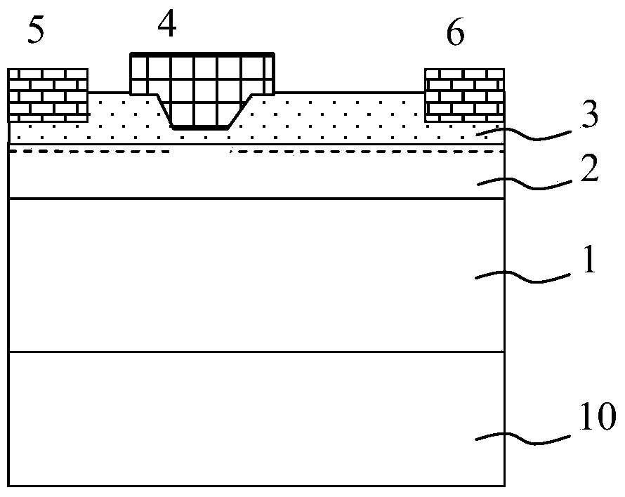
However, shallow fluorine ion implantation will cause a large number of fluorine ions to stay on the surface of GaN HEMT epitaxial layer, and the fluorine ions on the surface are not stable, and will cause fluorine ions to disperse under high temperature (>400°C) or high electric field conditions. migration, causing a shift in the device threshold voltage
In addition, fluorine ion implantation under normal implantation conditions will cause larger lattice damage in GaN devices, and the lattice damage will increase with the increase of implantation depth
If the fluorine ion implantation depth is increased under normal implantation conditions, the lattice damage will reach an irreversible level
Severe lattice defect scattering will reduce the mobility of channel carriers, reduce the saturation working current, and greatly restrict the working performance of the device

Method used


Image

  • Enhancement mode device based on fluoride ion injection and manufacturing method thereof
  • Enhancement mode device based on fluoride ion injection and manufacturing method thereof
  • Enhancement mode device based on fluoride ion injection and manufacturing method thereof

Examples


Embodiment Construction

[0044] The present invention will be described in detail below in conjunction with specific embodiments shown in the accompanying drawings. However, these embodiments do not limit the present invention, and any structural, method, or functional changes made by those skilled in the art according to these embodiments are included in the protection scope of the present invention.

[0045] Furthermore, repeated reference numerals or designations may be used in different embodiments. These repetitions are only for the purpose of simply and clearly describing the present invention, and do not represent any relationship between the different embodiments and / or structures discussed.

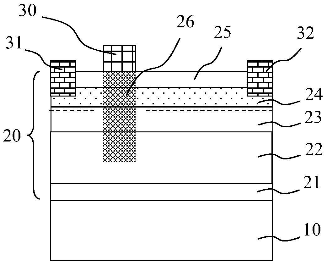
[0046] image 3 It is a schematic structural diagram of an enhanced device in the first embodiment of the present invention. Enhanced device of the present invention The enhanced device includes a substrate 10 , an epitaxial multilayer structure 20 formed on the substrate, and a gate 30 , a source 31 a...


PUM

PropertyMeasurementUnit
Growth temperatureaaaaaaaaaa

Abstract

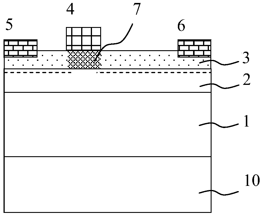
The invention discloses an enhancement mode device based on fluoride ion injection and a manufacturing method of the enhancement mode device based on fluoride ion implantation. The enhancement mode device based on fluoride ion injection comprises a substrate, an epitaxy multilayered structure formed on the substrate, a grid electrode, a source electrode and a drain electrode, wherein the grid electrode, the source electrode and the drain electrode are arranged on the epitaxy multilayered structure, and fluoride ions are injected in a heterogeneous structure layer below the grid electrode in a tunnel injection mode and are used for using up two-dimensional electron gas in the heterogeneous structure layer. As the fluoride ions are injected in the heterogeneous structure layer below the grid electrode in the tunnel injection mode and use up the two-dimensional electron gas in the heterogeneous structure layer below the grid electrode, the enhancement mode gallium nitride device is achieved. Meanwhile, unstable fluoride ions are removed through high temperature annealing, crystal lattices recover from damage caused when the fluoride ions are injected, and a crystalline state medium layer is utilized for protecting surfaces of nitride materials produced during high temperature annealing.

Description

technical field [0001] The invention relates to the technical field of microelectronics, in particular to an enhanced device based on fluorine ion implantation and a manufacturing method thereof. Background technique [0002] High Electron Mobility Transistor (HEMT) based on Gallium Nitride material is a strong competitor in the fields of RF / microwave power amplifiers and high temperature digital integrated circuits. It is based on the wide bandgap semiconductor material gallium nitride, which has the characteristics of high electron saturation drift speed, high breakdown field strength and good thermal conductivity of gallium nitride materials. Compared with silicon and gallium arsenide devices, It has obvious advantages in the application of high frequency, high voltage and high power. [0003] The core structure of HEMTs based on gallium nitride materials usually adopts AlGaN / GaN heterojunction, and there is a strong two-dimensional electron gas in the heterostructure, s...

Claims


Application Information

Patent Timeline
IPC IPC(8): H01L29/778H01L29/06H01L21/336
CPCH01L21/2654H01L29/66462H01L29/7786
Inventor 程凯陈洪维
Owner ENKRIS SEMICON
Learn More