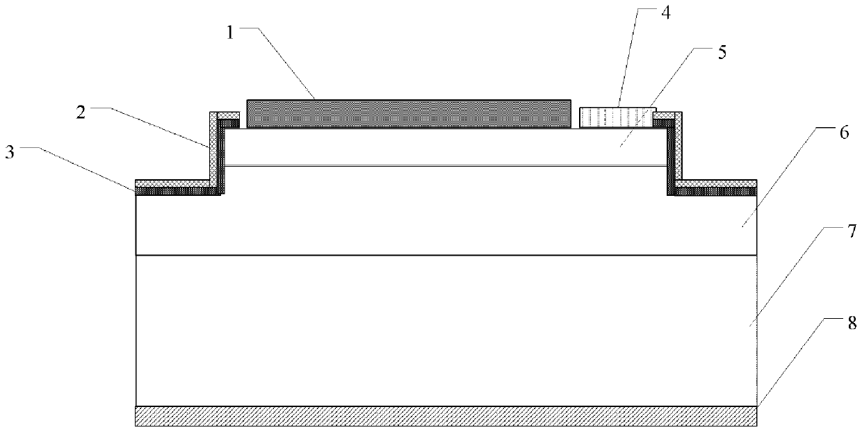
Manufacturing method of PIN-type isotope nuclear battery including niobium-doped n-type SiC epitaxial layer
An epitaxial layer and isotope technology, which is applied in the cross field of nuclear science and technology and microelectronics technology, can solve the problems of immature technology, low energy conversion efficiency, and small depletion region width, so as to improve the open circuit voltage and energy conversion efficiency, Effects of improving energy conversion efficiency and increasing the width of the depletion region
- Summary
- Abstract
- Description
- Claims
- Application Information
AI Technical Summary
Problems solved by technology
Method used
Image
Examples
Embodiment 1
[0035] Step 1: Epitaxial n-type epitaxial layer on SiC highly doped n-type substrate sample.
[0036] The selected doping concentration is 1×10 18 cm -3The highly doped n-type SiC substrate 7, after cleaning, is epitaxially grown on the highly doped n-type SiC substrate with a thickness of 4um and an initial n-type epitaxial layer doped with nitrogen ions, and its doping concentration is 1×10 15 cm -3 , the epitaxy temperature is 1570°C, the pressure is 100mbar, the reaction gas is silane and propane, the carrier gas is pure hydrogen, and the impurity source is liquid nitrogen.
[0037] Step 2: For a doping concentration of 1×10 15 cm -3 The initial n-type SiC epitaxial layer is implanted with niobium ions.
[0038] (2.1) For a doping concentration of 1×10 15 cm -3 The initial n-type SiC epitaxial layer was implanted with niobium ions, and the conditions of the niobium ion implantation were: the energy of ion implantation was 2200KeV, and the implantation dose was 5×10 ...
Embodiment 2
[0058] Step 1: Epitaxial n-type epitaxial layer on SiC highly doped n-type substrate sample.
[0059] The selected doping concentration is 5×10 18 cm -3 The highly doped n-type SiC substrate 7, after cleaning, is epitaxially grown on the highly doped n-type SiC substrate with a thickness of 3um and an initial n-type epitaxial layer doped with nitrogen ions, and its doping concentration is 5×10 15 cm -3 , the epitaxy temperature is 1570°C, the pressure is 100mbar, the reaction gas is silane and propane, the carrier gas is pure hydrogen, and the impurity source is liquid nitrogen.
[0060] Step 2: For a doping concentration of 5×10 15 cm -3 The initial n-type SiC epitaxial layer is implanted with niobium ions.
[0061] (2.1) For a doping concentration of 5×10 15 cm -3 The initial n-type SiC epitaxial layer was implanted with niobium ions, and the conditions of the niobium ion implantation were: the energy of ion implantation was 2000KeV, and the implantation dose was 1×10...
Embodiment 3
[0082] Step A: Epitaxial n-type epitaxial layer on SiC highly doped n-type substrate sample.
[0083] The selected doping concentration is 7×10 18 cm -3 The highly doped n-type SiC substrate 7, after cleaning, is epitaxially grown on the highly doped n-type SiC substrate with a thickness of 5um and an initial n-type epitaxial layer doped with nitrogen ions, and its doping concentration is 2×10 15 cm -3 , the epitaxy temperature is 1570°C, the pressure is 100mbar, the reaction gas is silane and propane, the carrier gas is pure hydrogen, and the impurity source is liquid nitrogen.
[0084] Step B: For a doping concentration of 2×10 15 cm -3 The initial n-type SiC epitaxial layer is implanted with niobium ions.
[0085] (B1) For a doping concentration of 2×10 15 cm -3 The initial n-type SiC epitaxial layer was implanted with niobium ions, and the conditions of the niobium ion implantation were: the energy of ion implantation was 2500KeV, and the implantation dose was 1×10 1...
PUM
| Property | Measurement | Unit |
|---|---|---|
| Thickness | aaaaa | aaaaa |
| Doping concentration | aaaaa | aaaaa |
| Doping concentration | aaaaa | aaaaa |
Abstract
Description
Claims
Application Information
 - R&D Engineer
- R&D Manager
- IP Professional
- Industry Leading Data Capabilities
- Powerful AI technology
- Patent DNA Extraction
Browse by: Latest US Patents, China's latest patents, Technical Efficacy Thesaurus, Application Domain, Technology Topic, Popular Technical Reports.
© 2024 PatSnap. All rights reserved.Legal|Privacy policy|Modern Slavery Act Transparency Statement|Sitemap|About US| Contact US: help@patsnap.com


