Polarization-state-controlled multimode-interference optical switch and manufacturing method thereof

A technology of multi-mode interference and polarization controller, applied in optics, nonlinear optics, optical waveguide coupling, etc., can solve the problems of high cost, complex structure, and difficult manufacturing process, and achieve low nonlinearity and high process difficulty , structure and modulation method simple effect

Active Publication Date: 2014-04-30
SOUTHEAST UNIV
View PDF4 Cites 1 Cited by
  • Summary
  • Abstract
  • Description
  • Claims
  • Application Information

AI Technical Summary

Problems solved by technology

The existing adjustable PLC-type optical switch mainly uses the principles of electro-optic effect, thermo-optic effect, magneto-optic effect, acousto-optic effect and other principles of the material, and needs to add a refractive index modulation module to change the refractive index of the multimode waveguide to realize the switch state adjustable. The production process is difficult, the structure is complex, and the cost is high

Method used


Image

  • Polarization-state-controlled multimode-interference optical switch and manufacturing method thereof
  • Polarization-state-controlled multimode-interference optical switch and manufacturing method thereof
  • Polarization-state-controlled multimode-interference optical switch and manufacturing method thereof

Examples


preparation example Construction

[0035] The preparation method of the above-mentioned multi-mode interference type optical switch controlled by polarization state comprises the following steps:

[0036] Step 10) Prepare a planar light wave optical circuit chip, specifically including step 101) to step 104):

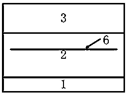
[0037]Step 101): Take a silicon wafer as the silicon substrate 1, clean the silicon wafer by wet chemical method, prepare a silicon dioxide buffer layer 2 on the silicon substrate 1 by thermal oxidation method, and use plasma-enhanced chemical vapor deposition method on the second Silicon oxide is doped with germanium dioxide to obtain a waveguide layer 3, and the difference between the thermal expansion coefficients of the waveguide layer 3 and the silicon dioxide buffer layer 2 is used to introduce cracks 6 in the silicon dioxide buffer layer 2 by controlling the thermal stress during the reaction process ;

[0038] Step 102): Prepare waveguide 4 on waveguide layer 3 by photolithography and etching pr...

Embodiment 1

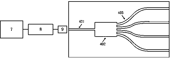
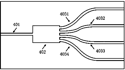
[0044] Such as figure 1 and figure 2 As shown, it is a polarization-controlled 1×4 multi-mode interference optical switch, including a planar light wave optical circuit chip, a light source and a polarization controller. The planar light wave optical circuit (PLC) chip includes a silicon substrate 1, a silicon dioxide buffer layer 2 grown on the silicon substrate 1, a waveguide 4 grown on the silicon dioxide buffer layer 2, and a cladding layer 5 grown on the waveguide 4 , there is a crack 6 in the silicon dioxide buffer layer 2 . The waveguide 4 includes an input-stage single-mode waveguide 401, an intermediate-stage multi-mode waveguide 402, a first output-stage single-mode waveguide 4031, a second output-stage single-mode waveguide 4032, a third output-stage single-mode waveguide 4033 and a fourth output-stage single-mode waveguide. Waveguide 4034. The light source is connected to the optical input end of the polarization controller, the optical output end of the polar...

Embodiment 2

[0046] The preparation method of the 1×4 multi-mode interference type optical switch controlled by polarization state is introduced below, so as to describe the above preparation method in more detail.

[0047] figure 1 The preparation method of the 1×4 multi-mode interference type optical switch controlled by the polarization state includes the following process:

[0048] Step 1): Fabricate a silicon dioxide buffer layer 2 and a waveguide 3 containing cracks 6 . refer to figure 2 As shown, it includes step 101), step 102) and step 103).

[0049] Step 101) Take a silicon wafer, use wet chemical method to clean the silicon wafer as the silicon substrate 1, and remove the dirt on the surface; then, after ultrasonic cleaning and drying with deionized water, the cleaning of the silicon wafer is completed;

[0050] Step 102) Prepare the silica buffer layer 2 containing cracks 6. There are many methods for preparing the silica buffer layer 2 containing cracks 6, such as chemica...


PUM

PropertyMeasurementUnit
lengthaaaaaaaaaa
widthaaaaaaaaaa
depthaaaaaaaaaa

Abstract

The invention discloses a polarization-state-controlled multimode-interference optical switch. The polarization-state-controlled multimode-interference optical switch comprises a planar optical wave and optical path chip, a light source, a polarization controller and an input fiber array. The planar optical wave and optical path chip comprises a silicon substrate, a silica buffer layer, waveguides and a covering layer. Cracks are formed in the silica buffer layer. The waveguides comprise an input-stage single-mode waveguide, an intermediate-stage multimode waveguide and an output-stage single-mode waveguide. The light source is connected with the optical input end of the polarization controller, and the optical output end of the polarization controller is connected with the input end of the input fiber array. The switch-on/off state of the multimode-interference optical switch is adjustable, and the multimode-interference optical switch has the advantages of thermal stabilization, low nonlinearity, low transmission loss, wide operation bandwidth and high integration and being capable of being efficiently coupled with a single-mode fiber, low in price, simple in structure, and the like. Meanwhile, the invention further discloses a manufacturing method of the polarization-state-controlled multimode-interference optical switch. The manufacturing method is simple, low in cost and capable of manufacturing the optical switch in batches.

Description

technical field [0001] The invention belongs to the technical field of integrated photonic devices, and in particular relates to a multi-mode interference optical switch controlled by polarization state and a preparation method thereof. Background technique [0002] The optical switch is a key device that can convert the channel of the optical signal in the optical transmission process, and can be widely used in the realization of functions such as routing selection, wavelength selection and optical cross-connection of the all-optical layer. According to the classification of the working medium, optical switches can be divided into free space optical switches and planar waveguide type (hereinafter referred to as: PLC type) optical switches. [0003] The PLC optical switch is manufactured by semiconductor technology, and has the advantages of compact structure, batch production, and high stability. Among them, the PLC-type optical switch based on silicon dioxide on silicon (...

Claims


Application Information

Patent Timeline
Patent Type & Authority Applications(China)
IPC IPC(8): G02F1/01G02B6/35
Inventor 孙小菡蒋卫锋戚健庭董纳陈源源
Owner SOUTHEAST UNIV
Why Eureka
Try Eureka