
Method for manufacturing back contact solar cell

A solar cell and back contact technology, applied in the field of solar cells, can solve the problems of difficult to produce back contact cells, complicated production process of back contact cells, high cost of photolithography, etc., so as to increase the effective semiconductor area, eliminate shading loss, The effect of short-circuit current improvement

Active Publication Date: 2014-05-14
JA SOLAR TECH YANGZHOU +1
View PDF4 Cites 37 Cited by
  • Summary
  • Abstract
  • Description
  • Claims
  • Application Information

AI Technical Summary

Problems solved by technology

However, the manufacturing process of back contact cells is relatively complicated, which includes multiple processes for making masks, which requires high alignment accuracy. In the past manufacturing methods, most of them use photolithography technology used in semiconductor integrated circuits. Make the mask of the back contact cell, but the cost of photolithography is very expensive, and it is currently difficult to apply to large-scale back contact cell production
Therefore, it has always been a great challenge to fabricate high-efficiency back-contact cells using a low-cost process flow.

Method used


Image

  • Method for manufacturing back contact solar cell
  • Method for manufacturing back contact solar cell
  • Method for manufacturing back contact solar cell

Examples


Embodiment 1

[0056] The preparation method of the back contact solar cell in the present embodiment comprises the following steps:

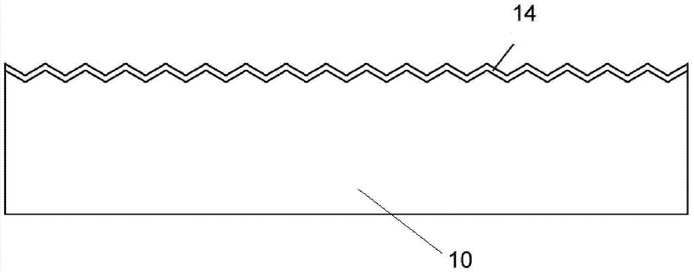
[0057] (1) The selected crystalline silicon substrate is a single crystal silicon substrate with (100) crystal orientation, figure 1 Given is an n-type CZ single crystal silicon substrate 10, the resistivity of which is 1-30Ω·cm, and the thickness of the silicon substrate is 50-300μm. For uneven suede, soak the silicon substrate with a mass concentration of 5-10% hydrochloric acid for 2 minutes, rinse the silicon substrate with deionized water, and deposit a very thin layer of PECVD on the front surface of the silicon substrate after drying. thin silicon oxide (SiO x ) thin film 14, the thickness of the thin film is 5-20nm, the refractive index is 1.4-1.6, and it acts as a diffusion buffer layer;

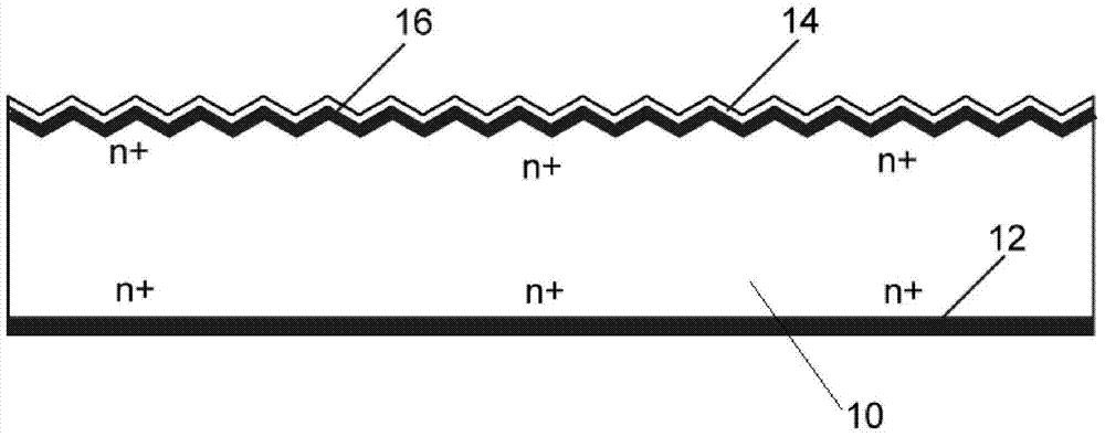
[0058] (2) if Figure 2A As shown, the well-plated SiO x The silicon substrate of the thin film 14 is put into an industrial tubular diffusion furnace for doub...

Embodiment 2

[0067] The preparation method of the back contact solar cell in the present embodiment comprises the following steps:

[0068] (1) The crystalline silicon substrate selected for the patent of this invention is a single crystal silicon substrate with (100) crystal orientation, figure 1 Provided is an n-type single crystal silicon substrate 10 with a volume resistivity of 1-30Ω·cm and a silicon substrate thickness of 50-300μm. The silicon substrate is placed in an aqueous solution of sodium hydroxide alcohol for surface corrosion to form unevenness The textured surface of the silicon substrate is soaked in hydrochloric acid with a mass concentration of 5-10% for 2 minutes, and then the silicon substrate is rinsed with deionized water. After drying, a thin layer is deposited on the front surface of the silicon substrate by PECVD. Silicon oxide (SiO x ) thin film 14, the thickness of the thin film is 5-20nm, the refractive index is 1.4-1.6, and its purpose is to serve as a diffus...


PUM

PropertyMeasurementUnit
Resistivityaaaaaaaaaa
Thicknessaaaaaaaaaa
Thicknessaaaaaaaaaa

Abstract

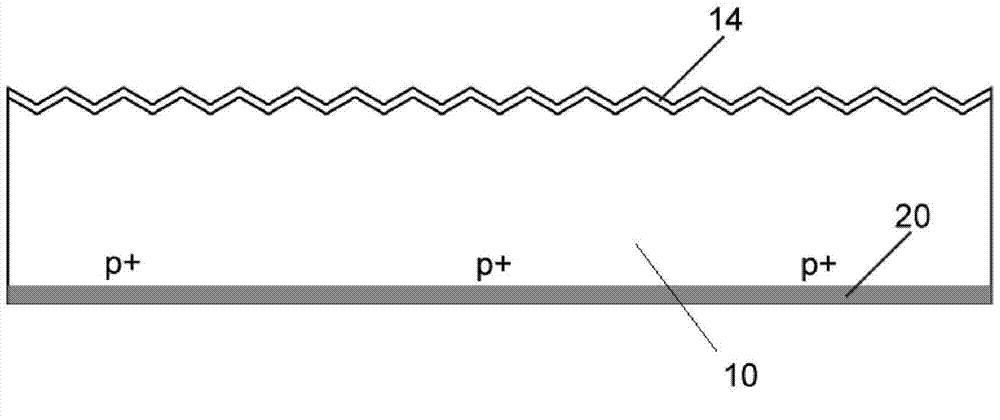
The invention discloses a method for manufacturing a back contact solar cell. According to the method, by means of the combination of the diffusion technology, the patterned dielectric mask technology, the etching technology, the laser insulation technology and the like, p+ doped regions and n+ doped regions which are mutually alternately ranked are manufactured on the back surface of a silicon substrate, band gaps for electric insulation of the p+ / n+ regions are manufactured at the joints of the p+ doped regions and the n+ doped regions, and an n+ front surface field FSF with the low surface doping concentration is manufactured on the front surface of the silicon substrate; the front surface and the back surface of the silicon substrate can be passivated and the front surface of the silicon substrate can be anti-reflected through SiOx, SiNx, AlOx and other dielectric films, and eventually the back contact solar cell is manufactured by achieving metallized contact between the p+ doped regions and the n+ doped regions on the back surface of the silicon substrate through the silk-screen printing process and the co-sintering process. The method for manufacturing the back contact solar cell and an existing process for producing a crystalline silicon solar cell have something in common, no new manufacturing equipment needs to be introduced, all manufacturing procedures can be finished on an existing industrial production line, and therefore cost is low, and the process is simple, reasonable, safe and reliable.

Description

technical field [0001] The invention belongs to the field of solar cells, and in particular relates to a preparation method of a back contact solar cell. Background technique [0002] A solar cell is a semiconductor device that converts light energy into electrical energy. Lower production costs and higher energy conversion efficiency have always been the goals pursued by the solar cell industry. For conventional solar cells, the p+ doped region contact electrodes and the n+ doped region contact electrodes are respectively located on the front and back sides of the battery sheet. The front of the battery is the light-receiving surface, and the coverage of the metal contact electrodes on the front will inevitably cause a part of the incident sunlight to be reflected by the metal electrodes, resulting in a part of optical loss. The coverage area of ​​the front metal electrode of an ordinary crystalline silicon solar cell is about 7%, and reducing the front coverage of the met...

Claims


Application Information

Patent Timeline
IPC IPC(8): H01L31/18
CPCH01L31/1804Y02E10/547Y02P70/50
Inventor 刘志锋尹海鹏张峰汤昆单伟
Owner JA SOLAR TECH YANGZHOU
Learn More