High-temperature nano-electrothermal film of double-film structure and preparation method thereof
A nano-electric heating film and double-layer film technology is applied in the field of semiconductor heating and infrared radiation, which can solve the problems of high power and low thermal efficiency, and achieve the effect of high safety factor, high thermal efficiency and shortening heating time.
- Summary
- Abstract
- Description
- Claims
- Application Information
AI Technical Summary
Problems solved by technology
Method used
Image
Examples
Embodiment 1
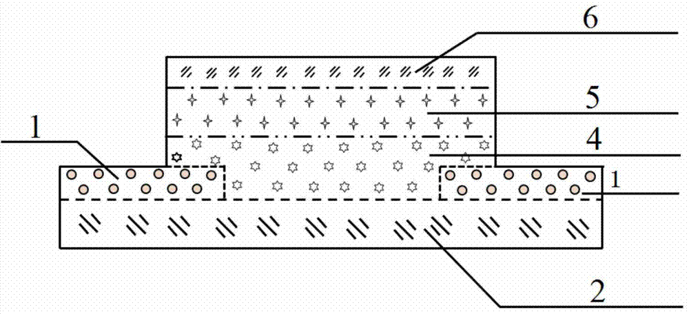
[0024] A high-temperature nanometer electric heating film with a double-layer film structure, such as figure 1 As shown, it consists of a platinum alloy thin film electrode 1, a quartz substrate 2, a silicon carbide film layer 4, and a molybdenum disilicide film layer 5. The quartz substrate is a high temperature resistant quartz plate or quartz tube, or is shaped as a curved high temperature resistant quartz substrate.
[0025] The preparation method of the high-temperature nanometer electrothermal film of double-layer film structure, its steps are as follows:
[0026] Substrate cleaning: The quartz substrate is cleaned with an ultrasonic cleaner with an ultrasonic frequency of 20-50KHz. It is first cleaned in deionized water, and then cleaned in the order of acetone, absolute ethanol, and deionized water. Each cleaning time is 10-50KHz. 15 minutes; then take out the quartz substrate, blow off the water droplets on the surface with an ear washing ball, put it into an electri...
Embodiment 2
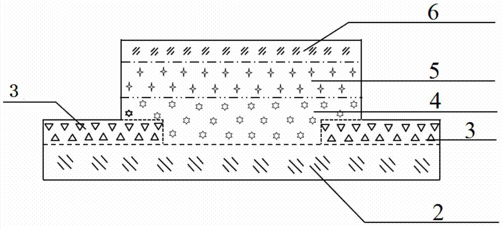
[0032] A high-temperature nanometer electric heating film with a double-layer film structure, such as figure 2 As shown, it consists of a cobalt-based alloy thin-film electrode 3 , a quartz substrate 2 , a silicon carbide film layer 4 , and a molybdenum disilicide film layer 5 . The quartz substrate is a high temperature resistant quartz plate or quartz tube, or is shaped as a curved high temperature resistant quartz substrate.
[0033] The preparation method of the high-temperature nanometer electrothermal film of double-layer film structure, its steps are as follows:
[0034] Substrate cleaning: The quartz substrate is cleaned with an ultrasonic cleaner with an ultrasonic frequency of 20-50KHz. It is first cleaned in deionized water, and then cleaned in the order of acetone, absolute ethanol, and deionized water. Each cleaning time is 10-50KHz. 15min. Then take out the substrate, blow off the water droplets on the surface with an ear washing ball, put it into an electric ...
PUM
| Property | Measurement | Unit |
|---|---|---|
| thermal efficiency | aaaaa | aaaaa |
Abstract
Description
Claims
Application Information


