Inorganic phase change photoresist and photolithographic technology based on inorganic phase change photoresist
An inorganic phase change and photolithography technology, which is applied in microlithography exposure equipment, photolithographic process exposure devices, photosensitive materials for optomechanical equipment, etc. Low etching and other problems, to achieve the effect of short production cycle, simple and convenient preparation method, and high yield
- Summary
- Abstract
- Description
- Claims
- Application Information
AI Technical Summary
Problems solved by technology
Method used
Image
Examples
Embodiment 1
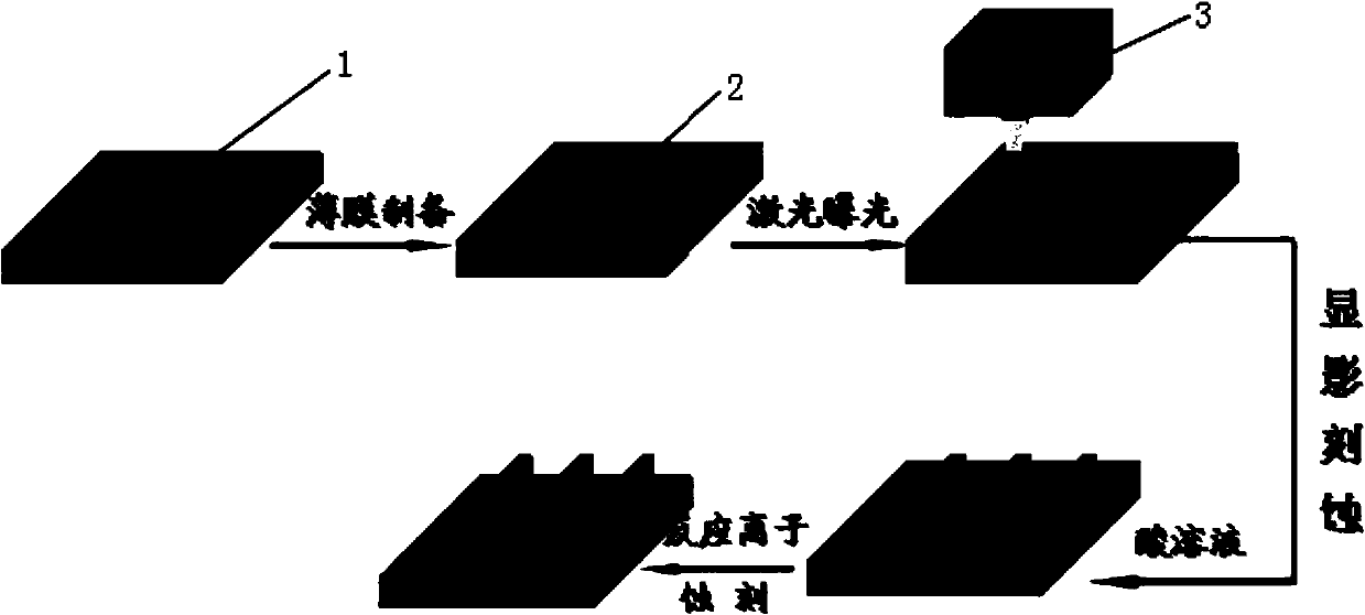
[0032] refer to figure 1 , is a flowchart of photolithography process steps.
[0033] Step a: Select silicon dioxide (SiO 2 ) as the substrate 1, using acetone, alcohol, and deionized water as cleaning agents, and ultrasonically cleaned for 10 minutes each in sequence. After cleaning, take it out and dry it with nitrogen gas, then dry it in a vacuum oven at 120°C for 1 hour, and take it out after cooling.
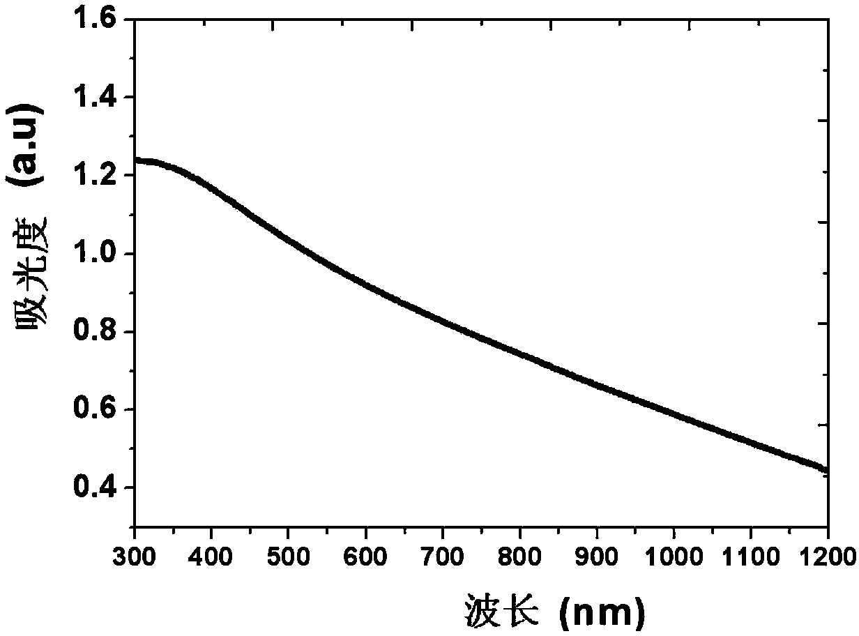
[0034] Step b: in the silicon dioxide (SiO 2 ) on the substrate 1 by magnetron sputtering to deposit a layer of high-etch-resistant amorphous film 2, that is, Ge 2 Sb 2(1-x) sn 2x Te 5 (0-5 Pa, the sputtering power is 50W, the argon (Ar) flow rate is 25sccm, the deposition pressure is 0.1Pa, the temperature of the substrate 1 is room temperature, the deposition time is 250s, and the obtained GSST thin film 2 has a thickness of 60nm. The surface morphology of the sample is as figure 2 As shown, very smooth with no large particles. image 3 It is the spectral absorpt...
Embodiment 2
[0040] Step a: Single crystal silicon (Si) is selected as the substrate 1, and other operations such as cleaning, drying, drying, and cooling are the same as step a of Embodiment 1.
[0041] Step b: On the monocrystalline silicon (Si) substrate 1 treated in the above step a, magnetron sputtering is used to deposit a layer of highly etch-resistant amorphous film 2, that is, Ge 2 Sb 2(1-x0 sn 2x Te 5 (0<x<0.3) amorphous film, hereinafter referred to as GSST film. The target material, deposition conditions and operation steps are the same as step b of Example 1.
[0042] Step c: Use laser 3 to write directly on the partial area of the thin film sample obtained in the above steps. The energy density and operation steps of laser 3 are the same as step c of Example 1.
[0043] Step d: put the GSST sample with micro / nano-scale pattern structure obtained in the above step c into a developing solution for development, and the developing solution and operation steps are the same a...
PUM
| Property | Measurement | Unit |
|---|---|---|
| thickness | aaaaa | aaaaa |
| surface roughness | aaaaa | aaaaa |
Abstract
Description
Claims
Application Information


