Organic electroluminescent device and preparation method thereof
An electroluminescent device and electroluminescent technology, which are applied in the directions of organic light-emitting devices, organic semiconductor devices, materials of organic semiconductor devices, etc., can solve the problems of low luminous efficiency of light-emitting devices, low HOMO energy level, and unfavorable industrial production, etc. The effect of reducing the probability of luminescence quenching of the device, improving the luminous efficiency, and increasing the transmission rate
- Summary
- Abstract
- Description
- Claims
- Application Information
AI Technical Summary
Problems solved by technology
Method used
Image

Examples
Embodiment 1
[0074] A method for preparing an organic electroluminescent device, comprising the following steps:
[0075] (1) Conductive anode substrate pretreatment
[0076] Sonicate the ITO substrate with a thickness of 100nm for 15 minutes with detergent and deionized water in order to remove organic pollutants on the glass surface.
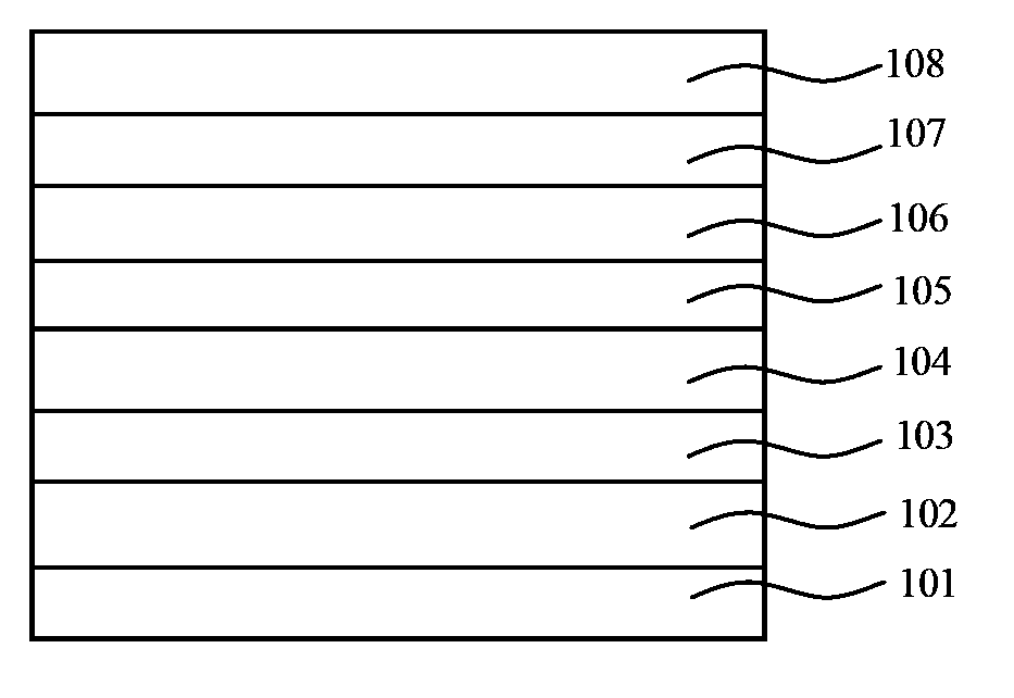
[0077] (2) Preparation of hole injection layer, hole transport layer, light emitting layer, hole blocking layer, electron transport layer, electron injection layer
[0078] Place the pretreated ITO substrate in a vacuum chamber (high vacuum coating system, Shenyang Scientific Instrument Development Center Co., Ltd.), and evacuate to 5×10 -3 Pa, MoO was deposited at a deposition rate of 1nm / s 3 Evaporated on the ITO substrate as a hole injection layer with a thickness of 30nm;
[0079] Evaporate TCTA on the hole injection layer as a hole transport layer at an evaporation rate of 1 nm / s, with a thickness of 40 nm;
[0080] 8-hydroxyquinoline aluminum (Al...
Embodiment 2
[0092] A method for preparing an organic electroluminescent device, comprising the following steps:
[0093] (1) Conductive anode substrate pretreatment
[0094] The AZO substrate with a thickness of 80nm was ultrasonicated for 15 minutes with detergent and deionized water in order to remove organic pollutants on the glass surface.
[0095] (2) Preparation of hole injection layer, hole transport layer, light emitting layer, hole blocking layer, electron transport layer, electron injection layer
[0096] Place the pretreated AZO substrate in a vacuum chamber (high vacuum coating system, Shenyang Scientific Instrument Development Center Co., Ltd.), and evacuate to 2×10 -4 Pa, WO was deposited at a deposition rate of 10nm / s 3 Evaporated on the AZO substrate as a hole injection layer with a thickness of 80nm;
[0097] N,N'-diphenyl-N,N'-bis(1-naphthyl)-1,1'-biphenyl-4,4'-diamine (NPB) was deposited at a deposition rate of 0.1nm / s Evaporated on the hole injection layer as a hol...
Embodiment 3
[0109] A method for preparing an organic electroluminescent device, comprising the following steps:
[0110] (1) Conductive anode substrate pretreatment
[0111] The IZO substrate with a thickness of 300nm was ultrasonicated for 15 minutes with detergent and deionized water in sequence to remove organic pollutants on the glass surface.
[0112] (2) Preparation of hole injection layer, hole transport layer, light emitting layer, hole blocking layer, electron transport layer, electron injection layer
[0113] Place the pretreated IZO substrate in a vacuum chamber (high vacuum coating system, Shenyang Scientific Instrument Development Center Co., Ltd.), and evacuate to 2.5×10 -3 Pa, MoO was deposited at a deposition rate of 5nm / s 3 Evaporated on the IZO substrate as a hole injection layer with a thickness of 40nm;
[0114] Evaporate TAPC on the hole injection layer as a hole transport layer at an evaporation rate of 0.5nm / s, and its thickness is 45nm;
[0115] Evaporate BCzVB...
PUM
| Property | Measurement | Unit |
|---|---|---|
| Thickness | aaaaa | aaaaa |
| Thickness | aaaaa | aaaaa |
| Thickness | aaaaa | aaaaa |
Abstract
Description
Claims
Application Information
 - R&D
- Intellectual Property
- Life Sciences
- Materials
- Tech Scout
- Unparalleled Data Quality
- Higher Quality Content
- 60% Fewer Hallucinations
Browse by: Latest US Patents, China's latest patents, Technical Efficacy Thesaurus, Application Domain, Technology Topic, Popular Technical Reports.
© 2025 PatSnap. All rights reserved.Legal|Privacy policy|Modern Slavery Act Transparency Statement|Sitemap|About US| Contact US: help@patsnap.com