A kind of passivation method of cadmium zinc telluride crystal surface
A crystal surface, cadmium zinc telluride wafer technology, applied in semiconductor devices, sustainable manufacturing/processing, electrical components, etc., can solve the problems of complexity, heating or ultraviolet irradiation, etc., to achieve low processing cost, no harsh processing conditions, Simple effect of passivation process
- Summary
- Abstract
- Description
- Claims
- Application Information
AI Technical Summary
Problems solved by technology
Method used
Image
Examples
Embodiment 1
[0021] A passivation method for a cadmium zinc telluride crystal surface, specifically comprising the steps of:
[0022] (1) Preparation of passivation solution
[0023] Wash the beaker 3 times with deionized water, slowly add 3.6g of thiourea into the beaker with 40g of deionized water, stir evenly to obtain passivation solution after all the thiourea is dissolved;
[0024] The above passivation solution is calculated by mass ratio, that is, thiourea: deionized water is 9:100;
[0025] (2), passivation treatment
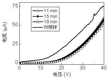
[0026] Put the cadmium zinc telluride wafer with the electrode prepared into the passivation solution obtained in step (1), soak for 11 minutes, and take out the cadmium zinc telluride wafer;
[0027] (3) Cleaning of CdZnTe wafer
[0028] Wash the CdZnTe wafers taken out in step (2) three times with deionized water, and then one time with absolute ethanol;
[0029] (4) Dry the CdZnTe wafer cleaned with absolute ethanol in step (3) with an ear cleaning ball to co...
PUM
 Abstract
Description
Claims
Application Information
