Check patentability & draft patents in minutes with Patsnap Eureka AI!

Bonding method based on multi-field coupling

A bonding and substrate technology, which is applied in the photolithographic process of pattern surface, precision positioning equipment, microstructure technology, etc., can solve the problems of affecting device performance, reducing bonding temperature, and low bonding reliability, etc., and achieves a wide range of applications. Application prospect, simple operation effect

Inactive Publication Date: 2014-07-16
河南省科学院应用物理研究所有限公司
View PDF10 Cites 11 Cited by
  • Summary
  • Abstract
  • Description
  • Claims
  • Application Information

AI Technical Summary

Problems solved by technology

Among them, silicon-silicon direct bonding and silicon-glass anodic bonding do not involve fillers, but the bonding temperature of the former is above 800 degrees Celsius, and the voltage of the latter is above 400V. This high temperature and high voltage environment often affects Device performance
The basic principle of solder bonding and metal-metal thermocompression bonding is to fill the surface of the two bonding substrates with solder or pure metal materials and then bond to reduce the bonding temperature. The former uses the low melting point of solder for bonding, but it is easy to Introduce pollution, and the bonding reliability is not high; the latter uses interdiffusion between atomic layers to achieve solid-state bonding in a hot-pressed environment, but the current hot-pressed bonding process is generally above 300 ° C and 10 MPa, which has a great impact on the life of the device. , reliability has a greater impact on

Method used


Image

  • Bonding method based on multi-field coupling

Examples


Embodiment Construction

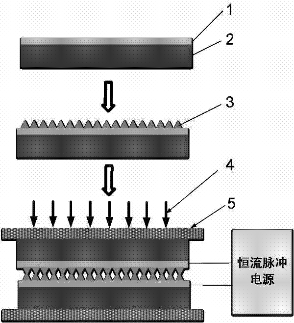
[0013] like figure 1 As shown, the main steps of the specific embodiment of the present invention include:

[0014] (1) The silicon substrate 2 is cleaned by a standard RCA process, and then metallic nickel 1 (Ni) is deposited on the substrate with a thickness of 500 nm by a sputtering process.

[0015] (2) The substrate prepared in (1) was degreased and derusted, and placed in the electroplating solution (copper sulfate pentahydrate 1.5 mol / L, copper nitrate 0.2 mol / L, ethylenediamine 2 mol / L, boric acid 0.3 mol / L, additives SPS15ppm, PEG1000ppm, JGB40ppm, solution temperature 30°C, pH value 5.0), the base material is used as the cathode, the copper plate or insoluble plate is used as the anode, and the base, copper plate and electroplating power supply form a loop through wires. A direct current (2A / dm2) is applied to the substrate by means of an electroplating power supply, and the electroplating time is 180 seconds to form a nano-metal needle-cone structure layer 3 .

...


PUM

PropertyMeasurementUnit
diameteraaaaaaaaaa

Abstract

The invention provides a bonding method based on multi-field coupling. The bonding method includes the steps that a metal film is prepared on a substrate to serve as a base, a nanometer metal needle cone structure is prepared on the surface of the metal base through an electrochemical deposition method to serve as a bonding layer, under the certain temperature and pressure conditions, the metal base is connected with a constant current pulse power supply, the power supply is switched off after a period of time, the metal base is kept for certain time under the constant temperature and pressure conditions, the current crowding and electromigration effects between nanometer interfaces are utilized, local joule heat is generated, diffusion among atoms is facilitated, and therefore low-temperature solid bonding can be achieved. The bonding method is simple in process and convenient to operate, process reliability is enhanced under the low temperature and pressure conditions, and the bonding method has application prospect in the fields of three-dimensional packaging, microsystem manufacturing and the like.

Description

technical field [0001] The invention belongs to the field of micro-nano system manufacturing, in particular to a bonding method based on multi-field coupling. Background technique [0002] With the development of microelectronics technology, the integration of circuits is getting higher and higher, the functions are more and more, and the device size is getting smaller and smaller, so that the electronic packaging technology is transitioning from two-dimensional to three-dimensional, thereby shortening the length of interconnection lines and reducing Electrical signal delay, improve device integration. Bonding is a key process for building a multi-layer chip structure and realizing three-dimensional packaging, and it is also a key link to ensure device performance and reliability. [0003] At present, in order to achieve reliable bonding between wafers, silicon-silicon direct bonding, silicon-glass anodic bonding, solder bonding, and metal-metal thermocompression bonding ha...

Claims


Application Information

Patent Timeline
Patent Type & Authority Applications(China)
IPC IPC(8): H01L21/02B81C3/00
CPCB81C3/001H01L21/0201
Inventor 宋晓辉乔彦超赵兰普庄春生岳鹏飞张萍
Owner 河南省科学院应用物理研究所有限公司
Features
  • R&D
  • Intellectual Property
  • Life Sciences
  • Materials
  • Tech Scout
  • Unparalleled Data Quality
  • Higher Quality Content
  • 60% Fewer Hallucinations
Learn More