Method for manufacturing epitaxy graphene back gate transistor with nitrogen-doped SiC substrate

A graphene back gate and transistor technology, applied in the field of graphene field effect transistors and their preparation, can solve the problems of complex process, easy damage and pollution of graphene, and achieve good electrical properties, expanded operating temperature range, and high electron mobility. Effect

Active Publication Date: 2014-07-23
江苏卓远半导体有限公司
View PDF7 Cites 1 Cited by
  • Summary
  • Abstract
  • Description
  • Claims
  • Application Information

AI Technical Summary

Problems solved by technology

The commonly used method of using graphene to prepare back gate transistors is: first thermally oxidize SiO on the surface of Si base 2 As a dielectric layer, the mask is subjected to photolithography, and after development, SiO is etched using reactive ion etching (RIE) technology. 2 , form

Method used


Image

  • Method for manufacturing epitaxy graphene back gate transistor with nitrogen-doped SiC substrate

Examples


Embodiment Construction

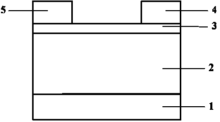
[0016] In the present invention, the gate and dielectric layer of the transistor are integrated with the SiC substrate through the method of implanting nitrogen ions, and then graphene is epitaxially grown on the SiC, and electrodes are plated to form a graphene transistor. details as follows:

[0017] Choose a 1 μm thick SiC substrate and clean it with a standard wafer cleaning method. The specific process is sonication with acetone, absolute ethanol, and deionized water for 5 to 10 minutes, ultrasonic power is 99%, and nitrogen is used after the ultrasonic. The gun will dry it quickly and put it in the sample box.

[0018] Hydrogen etching is used to remove impurities on the surface of the SiC substrate. The radio frequency induction heating furnace is selected as the etching device, the etching power is 400 W, and hydrogen gas (20 sccm, 30 s) is introduced to obtain a flat and uniform SiC substrate.

[0019] The nitrogen ions produced by a semiconductor ion implanter are used t...


PUM


Abstract

The invention discloses a method for manufacturing an epitaxy graphene back gate transistor with a nitrogen-doped SiC substrate. The method includes the steps of carrying out doping on the smooth and even SiC substrate through nitrogen ions generated through a semiconductor ion implantation machine, implanting the nitrogen ions with parameters ranging from 30 kev to 150 kev into the upper half portion of the SiC substrate to serve as a dielectric layer, implanting the nitrogen ions with parameters ranging from 500 kev to 1000 kev into the lower half portion of the SiC substrate to serve as a grid electrode, growing graphene on the SiC substrate with the implanted nitrogen ions in an epitaxy mode, and forming a graphene groove layer. According to the method, the transistor is manufactured directly through the SiC substrate, the grid electrode and the dielectric layer do not need to be deposited, operation is simple, and secondary pollution in the manufacturing process is avoided; the epitaxy-grown graphene is good in electrical property and has the high electron mobility.

Description

Technical field [0001] The invention relates to the technical field of field effect transistors, in particular to a graphene field effect transistor and a preparation method thereof. Background technique [0002] Graphene has various excellent properties with a specific surface area of ​​2630 , High carrier mobility is 200,000 , Is 100 times that of silicon, and the minimum resistivity is about 10 -6 Ω·cm, lower than copper and silver, high thermal conductivity of 5000 W , Is 10 times that of copper. Graphene is used for the preparation of transistors so that the transistors can work at room temperature. The commonly used method of using graphene to prepare back-gate transistors is to heat oxygen SiO on the surface of the Si substrate. 2 As the dielectric layer, the mask is subjected to photolithography, and after development, SiO is etched by reactive ion etching (RIE) technology 2 , Forming a trench with a width of 3~8 μm, and then transfer the prepared graphene to the subs...

Claims


Application Information

Patent Timeline
IPC IPC(8): H01L21/336
CPCH01L21/26506H01L29/66477
Inventor 王权邵盈任乃飞
Owner 江苏卓远半导体有限公司
Why Eureka
Try Eureka