
Method for improving electrical properties and optical properties of gallium nitride through laser irradiation on gallium nitride epitaxial wafer

A technology of laser irradiation and optical properties, applied in circuits, electrical components, semiconductor/solid-state device manufacturing, etc., can solve problems such as electrical and optical properties affecting the crystalline quality of materials, difficulty in epitaxial growth of GaN materials, and slow development of growth technology, etc. Accurate and controllable laser irradiation parameters, improved electro-optical properties, and no environmental pollution

Inactive Publication Date: 2014-07-30
BEIJING UNIV OF TECH
View PDF3 Cites 5 Cited by
  • Summary
  • Abstract
  • Description
  • Claims
  • Application Information

AI Technical Summary

Problems solved by technology

However, the lattice mismatch between the sapphire substrate and the GaN material is large, resulting in a large dislocation density in the epitaxially grown GaN material, which affects the crystal quality and many electrical and optical properties of the material.
It is precisely because of this that the epitaxial growth of high-quality GaN materials is very difficult, and the development of its growth technology is also very slow

Method used


Image

  • Method for improving electrical properties and optical properties of gallium nitride through laser irradiation on gallium nitride epitaxial wafer
  • Method for improving electrical properties and optical properties of gallium nitride through laser irradiation on gallium nitride epitaxial wafer
  • Method for improving electrical properties and optical properties of gallium nitride through laser irradiation on gallium nitride epitaxial wafer

Examples


Embodiment 1

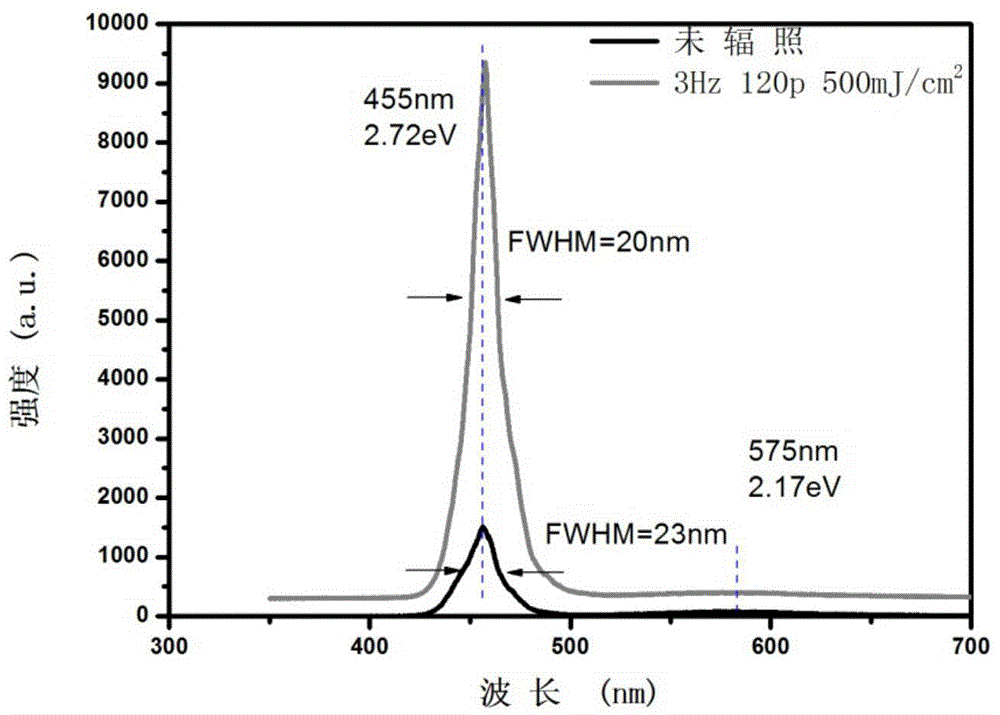
[0025] Cut the gallium nitride epitaxial wafer into square samples with a size of about 1cm×1cm each with a glass knife; immerse in acetone solvent for ultrasonic cleaning for 5 minutes, then rinse; immerse in alcohol solvent for ultrasonic cleaning for 5 minutes, then rinse; immerse in deionized water After ultrasonic cleaning for 6-10 minutes, rinse and dry. Place the pretreated GaN epitaxial wafer on the target stage, and irradiate it with an excimer laser with a wavelength of 248nm in an atmospheric environment; the pulse laser frequency is 3Hz, and the single pulse energy density is 0.5J / cm 2 , the number of pulses is 120. The out-of-focus amount is 4cm, and the compound eye structure is used to shape the outgoing laser light, and the spot area acting on the sample is 1cm 2 , that is, a square spot with a size of 1cm×1cm.

[0026] The photoluminescence spectra of the samples obtained through the above steps were compared with those of the unirradiated samples. The resu...

Embodiment 2

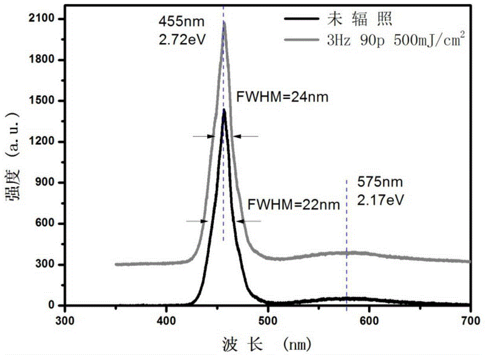
[0028] Cut the gallium nitride epitaxial wafer into square samples with a size of about 1cm×1cm each with a glass knife; immerse in acetone solvent for ultrasonic cleaning for 5 minutes, then rinse; immerse in alcohol solvent for ultrasonic cleaning for 5 minutes, then rinse; immerse in deionized water After ultrasonic cleaning for 6-10 minutes, rinse and dry. Place the pretreated gallium nitride epitaxial wafer on the target stage, and irradiate it with an excimer laser with a wavelength of 248nm in an atmospheric environment; the pulse laser frequency is 3Hz, and the single pulse energy density is 0.5J / cm 2 , the number of pulses is 90. The out-of-focus amount is 4cm, and the compound eye structure is used to shape the outgoing laser light, and the spot area acting on the sample is 1cm 2 , that is, a square spot with a size of 1cm×1cm.

[0029]The photoluminescence spectra of the samples obtained through the above steps were compared with those of the unirradiated samples....

Embodiment 3

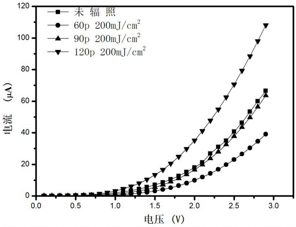
[0031] Cut the gallium nitride epitaxial wafer into square samples with a size of about 1cm×1cm each with a glass knife; immerse in acetone solvent for ultrasonic cleaning for 5 minutes, then rinse; immerse in alcohol solvent for ultrasonic cleaning for 5 minutes, then rinse; immerse in deionized water After ultrasonic cleaning for 6-10 minutes, rinse and dry. Place the pretreated GaN epitaxial wafer on the target stage, and irradiate it with an excimer laser with a wavelength of 248nm in an atmospheric environment; the pulse laser frequency is 3Hz, and the samples are irradiated with different single pulse energies and pulse numbers. Irradiate. At a single pulse energy density of 0.2J / cm 2 In the case of , the samples were irradiated with pulse numbers of 60, 90, and 120, respectively. When the number of pulses is 120, the single pulse energy density is 0.2J / cm 2 , 0.15J / cm 2 The sample is irradiated. The out-of-focus amount is 4cm, and the compound eye structure is used...


PUM


Abstract

The invention discloses a method for improving the electrical properties and the optical properties of gallium nitride through laser irradiation on a gallium nitride epitaxial wafer and belongs to the field of preparation of materials. According to the method, first, the GaN epitaxial wafer is preprocessed, contaminated attachments, organic residue and the like on the surface of the GaN epitaxial wafer are removed, surface lattice defects are overcome, a 248-nm excimer laser is adopted for irradiating the GaN epitaxial wafer, the single pulse energy density ranges from 0.15 J / cm<2> to 0.6 J / cm<2>, through test, the photoluminescence of the irradiated sample changes remarkably, the defect luminescence peak strength in the position of 455 nm (2.72 eV) is the highest and increased obviously compared with that of the GaN epitaxial wafer before irradiation, the defect luminescence peak strength can be six times that of the GaN epitaxial wafer before irradiation to the maximum extent, and all those can be attributed to the counterdiffusion phenomenon and the surface recystallization effect of surface atoms of the sample. A magnetron sputtering method is adopted for deposition of Ni(30 nm) / Au (100 nm) metal electrodes on the surface of the sample, then, the carrier concentration, the surface resistivity and the like are tested, and the result shows that the ohmic contact of the sample is improved to a certain extent after irradiation.

Description

technical field [0001] The invention belongs to the field of material preparation. Background technique [0002] As an emerging material with rich physical properties, wide bandgap semiconductors represented by materials such as gallium nitride and silicon carbide are playing an increasingly important role in current production and life. Especially in recent years, blue LEDs based on GaN have developed rapidly. [0003] The bandgap of GaN material is direct bandgap type, and its bandgap width is 3.39eV at room temperature, which belongs to the category of wide bandgap semiconductors, and generally has a high quantum efficiency during carrier recombination. The GaN material has a direct band gap, which means that it has a wide band gap, and is very suitable for making blue, green and ultraviolet light-emitting devices (such as LEDs) and ultraviolet light detection devices. Its electron saturation rate, breakdown electric field, thermal conductivity, and band gap are higher ...

Claims


Application Information

Patent Timeline
Patent Type & Authority Applications(China)
IPC IPC(8): H01L21/268
CPCH01L21/268
Inventor 蒋毅坚谈浩琪赵艳
Owner BEIJING UNIV OF TECH
Learn More