Micro-nano orderly through-hole array metal film sensor based on piezoelectric substrate sheet and manufacturing method thereof

A piezoelectric substrate and metal film technology, applied in the field of sensors, can solve problems such as pattern distortion, and achieve the effect of reducing transfer printing, good elasticity and low hardness

Active Publication Date: 2014-08-20
SUN YAT SEN UNIV
View PDF7 Cites 16 Cited by
  • Summary
  • Abstract
  • Description
  • Claims
  • Application Information

AI Technical Summary

Problems solved by technology

However, PDMS soft stamps are prone to graphic distortion during use

Method used


Image

  • Micro-nano orderly through-hole array metal film sensor based on piezoelectric substrate sheet and manufacturing method thereof
  • Micro-nano orderly through-hole array metal film sensor based on piezoelectric substrate sheet and manufacturing method thereof
  • Micro-nano orderly through-hole array metal film sensor based on piezoelectric substrate sheet and manufacturing method thereof

Examples


Embodiment 1

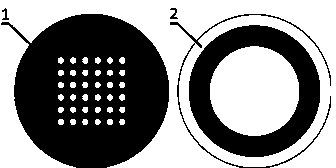
[0038] Such as Figure 1-2 As shown, the present invention is based on the micro-nano ordered through-hole array metal thin film sensor based on the piezoelectric substrate sheet. , the upper and lower metal films are attached to both sides of the quartz crystal plate,

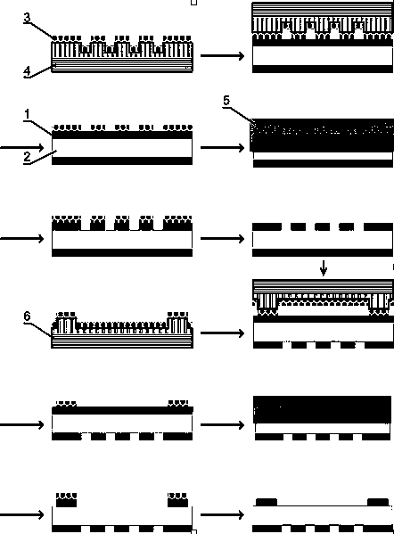
[0039] Such as image 3 , a preferred implementation example of the present invention comprises the following steps:

[0040] S1: Make a composite elastic stamp, the detailed process is as follows.

[0041] Using photolithography technology on the silicon wafer, the ordered micro-nano column array template and the ring pattern template are prepared as the original template for further replicating the composite elastic stamp.

[0042] Drop the mixed PDMS (component A:B=1:3) prepolymer on the original template with a pipette, and set the parameters of the spin coater as follows: slow rotation at 600 rpm for 18 s, fast rotation at 3000 rpm 60 s. The spin-coated template was heated at 70 °...


PUM


Abstract

The invention relates to a micro-nano orderly through-hole array metal film sensor based on a piezoelectric substrate sheet. The micro-nano orderly through-hole array metal film sensor structurally comprises a micro-nano orderly through-hole array metal film, the piezoelectric substrate sheet and an annular metal film from top to bottom, wherein the substrate is made of piezoelectric quartz crystals or piezoelectric ceramic. A manufacturing method is further provided. According to the manufacturing method, micro-nano orderly array patterns and annular patterns are machined on a silicon wafer through photoetching, and then a composite stamp with a hard PDMS (A:B=1:3) pattern layer and an elastic PDMS (A:B=1:10) substrate layer is copied through polydimethylsiloxane (PDMS, obtained by mixing the component A and the component B); thiol ink is smeared on the surface of the stamp, the stamp is pressed on the piezoelectric substrate plated with a gold film, and then anti-corrosion patterns of a compact thiol monomolecular layer is formed through self assembly; a porous gold film and an annular gold film are manufactured through wet method etching. The micro-nano orderly through-hole array metal film sensor can be applied to the field of combined sensing through the optical abnormal transmission technology, the quartz crystal microbalance technology and the electrochemistry technology and other fields. The manufacturing method has the advantages of being easy and convenient to perform, low in cost, controllable, high in repeatability and the like.

Description

technical field [0001] The invention relates to a sensor, in particular to a metal thin film sensor based on a piezoelectric substrate sheet with an array of micro-nano ordered through-holes and a manufacturing method thereof. Background technique [0002] The micro-nano ordered through-hole array metal film based on the piezoelectric substrate sheet has a wide range of applications in the fields of physical, chemical and biological sensing. On the one hand, the micro-nano ordered through-hole array has surface plasmon resonance effect, and the optical transmittance at a specific wavelength is higher than the ratio of the hole area to the total area, which can be used for photoelectric detection and chemical and biological refractive index sensing based on optical anomalous transmission. . Porous metal membranes have high specific surface area, excellent electrical conductivity and stable chemical properties, and can be used as working electrodes in electrochemical methods....

Claims


Application Information

Patent Timeline
Patent Type & Authority Applications(China)
IPC IPC(8): B81B7/02B81C1/00G01N21/59G01N5/00G01N27/26
Inventor 周建华李万博江雪芹
Owner SUN YAT SEN UNIV
Why Eureka
Try Eureka