
AlN film growing on Cu substrate and preparing method and application of AlN film

A substrate and thin film technology, applied in the field of AlN thin film and its preparation, can solve the problems affecting the quality of epitaxial thin film growth, unstable chemical properties of metal Cu substrate, difficult thin film epitaxy, etc. The effect of small width value and lower growth temperature

Active Publication Date: 2014-08-20
广州市艾佛光通科技有限公司
View PDF3 Cites 0 Cited by
  • Summary
  • Abstract
  • Description
  • Claims
  • Application Information

AI Technical Summary

Problems solved by technology

[0005] However, the chemical properties of the metal Cu substrate are unstable. When the epitaxial temperature is higher than 700 ° C, the interface reaction between the epitaxial nitride and the metal Cu substrate will seriously affect the quality of the epitaxial film growth.
Pioneering researcher and well-known scientist Akasaki et al. have tried to apply traditional MOCVD or MBE technology to directly epitaxially grow nitrides on substrate materials with variable chemical properties. difficulty

Method used


Image

  • AlN film growing on Cu substrate and preparing method and application of AlN film
  • AlN film growing on Cu substrate and preparing method and application of AlN film
  • AlN film growing on Cu substrate and preparing method and application of AlN film

Examples


Embodiment 1

[0035] A method for preparing an AlN thin film grown on a Cu substrate, comprising the following steps:

[0036] (1) Selection of the substrate and its crystal orientation: Cu substrate is used, and the (111) plane is 0.5° away from the (100) direction as the epitaxial plane. The crystal epitaxial orientation relationship is: the (0001) plane of AlN is parallel to the ( 111) Surface.

[0037] (2) Substrate surface polishing, cleaning and annealing treatment: firstly, the Cu substrate surface is polished with diamond slurry, and the substrate surface is observed with an optical microscope until there are no scratches, and then the chemical mechanical polishing method is used for polishing ; Secondly, put the Cu substrate in deionized water and ultrasonically clean it at room temperature for 3 minutes to remove the dirt particles on the surface of the Cu substrate, then wash it with acetone and ethanol in order to remove the surface organic matter, and dry it with high-purity dr...

Embodiment 2

[0046] A method for preparing an AlN thin film grown on a Cu substrate, comprising the following steps:

[0047] (1) Selection of the substrate and its crystal orientation: Cu substrate is used, and the (111) plane is 1° away from the (100) direction as the epitaxial plane. The crystal epitaxial orientation relationship is: the (0001) plane of AlN is parallel to the ( 111) Surface.

[0048] (2) Substrate surface polishing, cleaning and annealing treatment: firstly, the surface of the Cu substrate is polished with diamond slurry, and the surface of the substrate is observed with an optical microscope until there are no scratches, and then the method of chemical mechanical polishing is used for polishing ; Secondly, put the Cu substrate in deionized water and ultrasonically clean it at room temperature for 5 minutes to remove the dirt particles on the surface of the Cu substrate, then wash it with acetone and ethanol in order to remove the surface organic matter, and dry it with...


PUM

PropertyMeasurementUnit
thicknessaaaaaaaaaa
thicknessaaaaaaaaaa
thicknessaaaaaaaaaa

Abstract

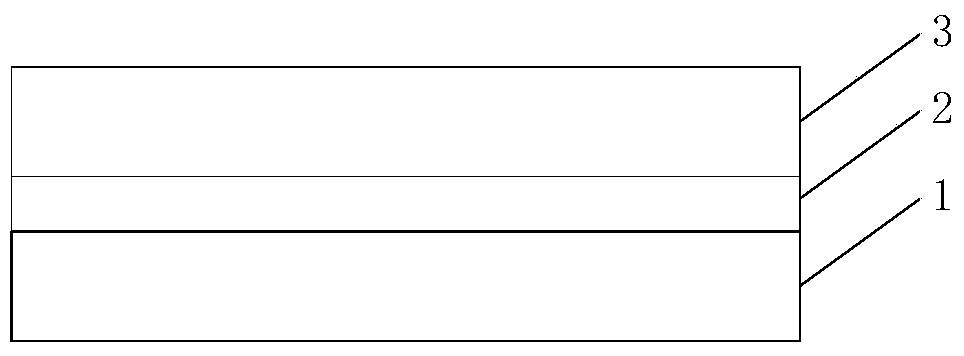
The invention discloses an AlN film growing on a Cu substrate. The AlN film growing on the Cu substrate is characterized by comprising the Cu substrate, an AlN buffer layer and an AlN film body, the AlN buffer layer grows on the Cu substrate, and the AlN film body grows on the AlN buffer layer; the face (111) deviating towards the direction of the face (100) by 0.5 to 1 degree serves as an epitaxial face of the Cu substrate. The invention further discloses the AlN film growing on the Cu substrate and a preparing method of the AlN film. The AlN film grows through the pulsed laser deposition technical growth technology and due to the fact that large kinetic energy can be provided for a precursor of the film through pulsed laser radiation, the growth temperature of the AlN film can be reduced to a great degree; in addition, due to the low temperature, the interfacial reaction between an epitaxial layer and the substrate is restrained, an important guarantee is provided for epitaxial growth of the AlN film on the metal Cu substrate, and the AlN film which has good crystalline quality and grows on the Cu substrate is obtained.

Description

technical field [0001] The invention relates to an AlN thin film, in particular to an AlN thin film grown on a Cu substrate and its preparation method and application. Background technique [0002] AlN is a group III compound, which generally exists in the wurtzite structure in the hexagonal system, and has many excellent properties, such as high thermal conductivity, low thermal expansion coefficient, high electrical insulation properties, and high dielectric breakdown strength. , excellent mechanical strength, excellent chemical stability and low toxicity, good optical properties, etc. Because AlN has many excellent properties, such as wide band gap, strong polarization, and a band gap of 6.2eV, it is widely used in electronic devices, integrated circuit packaging, optical films and heat dissipation devices. [0003] AlN thin films must have high crystal quality in order to meet the above various applications. At present, most AlN thin film devices are grown on sapphire ...

Claims


Application Information

Patent Timeline
Patent Type & Authority Applications(China)
IPC IPC(8): H01L21/205H01L33/00H01L33/02H01L31/18H01L31/0248
CPCH01L21/02425H01L21/02458H01L21/0254H01L21/0262H01L29/06H01L31/1852H01L31/1856H01L33/0066H01L33/0075Y02P70/50
Inventor 李国强
Owner 广州市艾佛光通科技有限公司
Learn More