Silicon-based ferroelectric grid thin film transistor and preparation method thereof

A technology of thin-film transistors and transistors, applied in transistors, semiconductor/solid-state device manufacturing, circuits, etc., can solve problems such as incompatibility, high price, and restrictions on the application and development of ferroelectric gate thin-film transistors, and achieve low turn-on voltage and low cost , easy process compatible effect

Inactive Publication Date: 2014-08-20
XIANGTAN UNIV
View PDF4 Cites 10 Cited by
  • Summary
  • Abstract
  • Description
  • Claims
  • Application Information

AI Technical Summary

Problems solved by technology

However, these special oxide single crystal substrates are not only expensive, but also incompatible with the current mainstream integrated circuit process, i.e. silicon proc

Method used


Image

  • Silicon-based ferroelectric grid thin film transistor and preparation method thereof
  • Silicon-based ferroelectric grid thin film transistor and preparation method thereof
  • Silicon-based ferroelectric grid thin film transistor and preparation method thereof

Examples


Embodiment 1

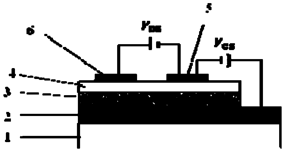
[0044] In this example, LaNiO was prepared on a Si(100) substrate with an offcut angle θ of 6° in the [100] direction by pulsed laser deposition. 3 Thin film as bottom gate electrode, Bi 3.15 Nd 0.85 Ti 3 o 12 A ferroelectric gate thin film transistor with a ferroelectric thin film as an insulating layer and a ZnO thin film as an active layer, comprising the following steps:

[0045] (1) Installation of substrate and target

[0046] In a vacuum chamber, the LaNiO 3 、 Bi 3.15 Nd 0.85 Ti 3 o 12 and the ZnO target are installed on the multi-target rack, and the obliquely cut Si substrate is cleaned and installed on the substrate rack so that the direction of the laser beam is aligned with the LaNiO 3 For the target, adjust the distance between the substrate and the target to 87mm.

[0047] (2) vacuuming

[0048] Turn on the mechanical pump and the molecular pump in sequence to pump the pressure in the vacuum chamber to 5×10 -8 Torr.

[0049] (3)Laser coating

[0050...

Embodiment 2

[0057] In this example, LaNiO was prepared on a Si(001) substrate with an off-cut angle θ of 6° in the [100] direction by pulsed laser deposition. 3 Thin film as bottom gate electrode, Pb(Zr 0.53 Ti 0.47 )O 3 A ferroelectric gate thin film transistor with a ferroelectric thin film as an insulating layer and a ZnO thin film as an active layer, comprising the following steps:

[0058] (1) Installation of substrate and target

[0059] The selected ferroelectric material target is Pb(Zr 0.53 Ti 0.47 )O 3 Target material, all the other are the same as embodiment 1.

[0060] (2) vacuuming

[0061] Same as Example 1

[0062] (3)Laser coating

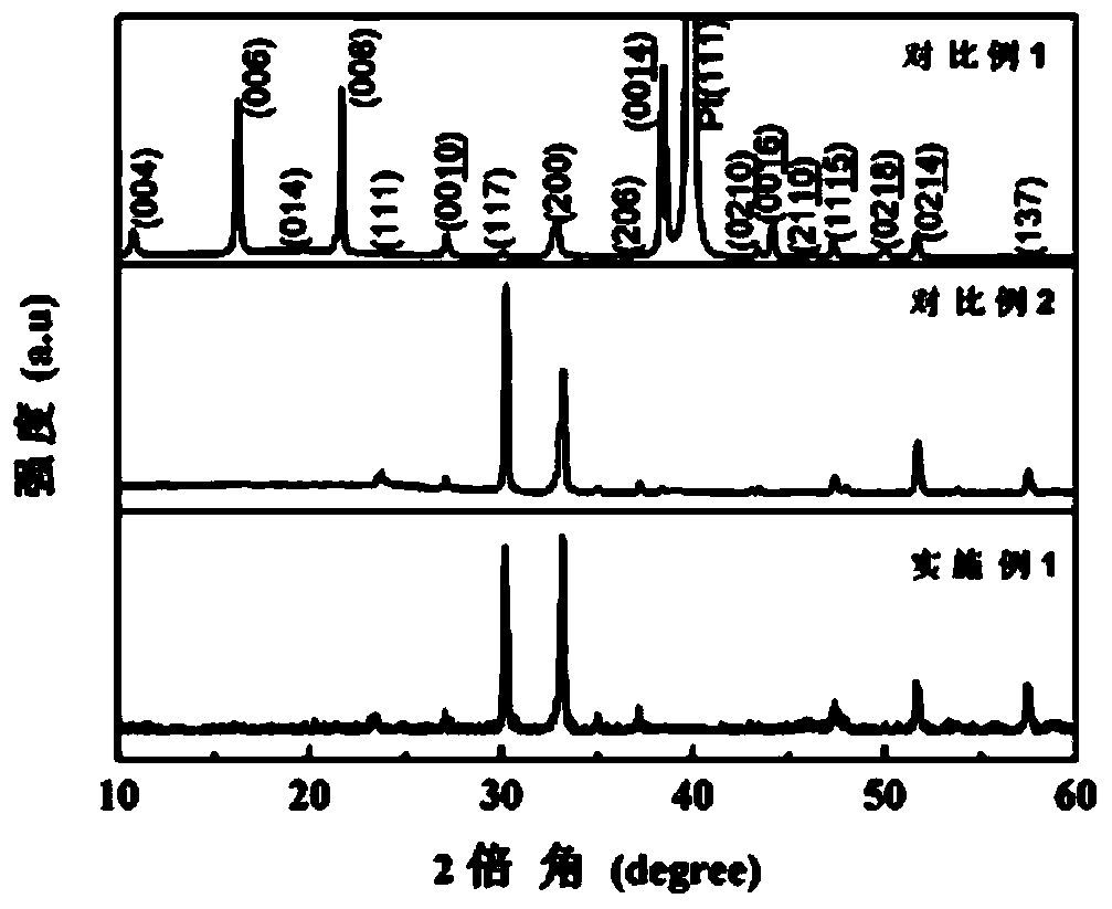
[0063] NeO 3 The deposited oxygen pressure is 50mTorr, resulting in highly c-axis oriented LaNiO 3 Thin film, its thickness is 50nm; Pb(Zr 0.53 Ti 0.47 )O 3 The deposition oxygen pressure of the ferroelectric thin film is 100mTorr, and the deposition temperature is 600°C, and the Pb(Zr 0.53 Ti 0.47 )O 3 Ferroelectric layer thin...

Embodiment 3

[0067] In this example, LaNiO was prepared on a Si(100) substrate with an offcut angle θ of 5° in the [110] direction by pulsed laser deposition. 3 Thin film as bottom gate electrode, Bi 3.25 La 0.75 Ti 3 o 12 Ferroelectric thin film as insulating layer, In 2 o 3 : Sn thin film is used as the ferroelectric gate thin film transistor of active layer, comprises the following steps:

[0068] (1) Installation of substrate and target

[0069] The selected ferroelectric material target and oxide semiconductor target are Bi 3.25 La 0.75 Ti 3 o 12 Target and In 2 o 3 : Sn target material, all the other are with embodiment 1.

[0070] (2) vacuuming

[0071] Same as Example 1

[0072] (3)Laser coating

[0073] Bi 3.25 La 0.75 Ti 3 o 12The deposition oxygen pressure of the ferroelectric thin film is 250mTorr, the deposition temperature is 750℃, and the Bi with a-axis preferred orientation is obtained. 3.25 La 0.75 Ti 3 o 12 Ferroelectric thin film, its thickness is ...


PUM

PropertyMeasurementUnit
Bevel angleaaaaaaaaaa
Thicknessaaaaaaaaaa
Thicknessaaaaaaaaaa

Abstract

The invention discloses a silicon-based ferroelectric grid thin film transistor and a preparation method thereof. A beveled mono-crystalline silicon substrate (1) serves as the bottom layer of the transistor, a perovskite conductive oxide bottom grid electrode (2), a ferroelectric insulating layer (3) and an oxide semiconductor active layer (4) are sequentially formed on the middle layer from bottom to top and a transistor source electrode (5) and a drain electrode (6) are arranged on the top layer of the transistor, wherein the beveled mono-crystalline silicon substrate (1) is intrinsic silicon with a step in the size of that of an atom. The ferroelectric grid thin film transistor is a non-volatile storage device, has the advantages of high radiation resistance, high reading and writing speed, low power consumption and the like of a ferroelectric random access memory, and further has the advantages that the starting voltage is low, the switch ratio is high, the device structure is simple, the preparation technology is simpler, low in cost and prone to being compatible with an existing silicon technology, and an all-epitaxial structure can be realized.

Description

technical field [0001] The invention belongs to the technical field of non-volatile memory in the microelectronics industry, and specifically relates to a silicon-based ferroelectric gate thin film transistor and a preparation method thereof. Background technique [0002] Ferroelectric memory has the advantages of non-volatility, low power consumption, high read and write speed, high storage density, strong radiation resistance, etc., and has very broad application prospects in the fields of electronic information and national defense. The currently commercialized ferroelectric RAM is mainly 1T1C structure ferroelectric memory based on ferroelectric capacitors, which has problems such as destructive readout, large cell size, and low integration. [0003] The ferroelectric gate thin film transistor uses a ferroelectric layer to replace the insulating layer (such as SiO2) in ordinary thin film transistors. 2 , HfO 2 ) and prepared 1T structure non-volatile ferroelectric memo...

Claims


Application Information

Patent Timeline
IPC IPC(8): H01L29/786H01L21/34H01L21/285
CPCH01L29/786H01L21/285H01L29/401H01L29/66969
Inventor 钟向丽丁涛张溢宋宏甲王金斌周益春
Owner XIANGTAN UNIV
Why Eureka
Try Eureka