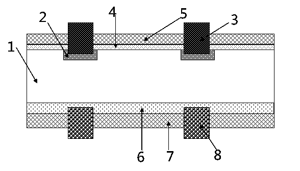
N-type crystalline silicon two-sided battery and preparing method thereof
A double-sided cell and crystalline silicon technology, applied in the field of solar cells, can solve the problems of complex preparation methods and high preparation costs of double-sided cells, and achieve the effects of improving stability, simplifying manufacturing processes, and increasing short-circuit current density.
- Summary
- Abstract
- Description
- Claims
- Application Information
AI Technical Summary
Problems solved by technology
Method used
Image
Examples
Embodiment 1
[0035] A method for preparing an N-type crystalline silicon double-sided battery, comprising the following steps:
[0036] 1) Chemical cleaning
[0037] For the surface texture of the N-type silicon substrate with a resistivity of 0.3Ω·cm, a pyramid-shaped light-trapping structure is prepared on the surface of the substrate with dilute sodium hydroxide or potassium hydroxide solution, and then dilute hydrochloric acid and hydrogen Cleaning with hydrofluoric acid to obtain a chemically cleaned N-type silicon substrate;
[0038] 2) Boron doped layer printed on the upper surface
[0039] A boron-doped layer is printed on the upper surface of the chemically cleaned N-type silicon substrate. The shape of the printed boron-doped layer matches the cross-sectional shape of the positive electrode of the battery. After printing, it is dried in a drying oven at 400 ° C to obtain N-type silicon substrate with boron source;
[0040] 3) The lower surface is implanted with phosphorus sour...
Embodiment 2
[0052] A method for preparing an N-type crystalline silicon double-sided battery, comprising the following steps:
[0053] 1) Chemical cleaning
[0054] For the surface texture of the N-type silicon substrate with a resistivity of 10Ω·cm, use dilute sodium hydroxide or potassium hydroxide solution to prepare a pyramid-shaped light-trapping structure on the surface of the substrate, and then use diluted hydrochloric acid and hydrofluoric acid to Acid cleaning to obtain a chemically cleaned N-type silicon substrate;
[0055] 2) Boron doped layer printed on the upper surface
[0056] A boron-doped layer is printed on the upper surface of the chemically cleaned N-type silicon substrate. The shape of the printed boron-doped layer matches the cross-sectional shape of the positive electrode of the battery. After printing, it is dried in a drying oven at 400 ° C to obtain N-type silicon substrate with boron source;
[0057] 3) The lower surface is implanted with phosphorus source a...
Embodiment 3
[0069] A method for preparing an N-type crystalline silicon double-sided battery, comprising the following steps:
[0070] 1) Chemical cleaning
[0071] For the surface texture of the N-type silicon substrate with a resistivity of 0.3Ω·cm, a pyramid-shaped light-trapping structure is prepared on the surface of the substrate with dilute sodium hydroxide or potassium hydroxide solution, and then dilute hydrochloric acid and hydrogen Cleaning with hydrofluoric acid to obtain a chemically cleaned N-type silicon substrate;
[0072] 2) Boron source implanted on the upper surface
[0073] Implant a boron source on the upper surface of the chemically cleaned N-type silicon substrate, and in the case of ion beam energy 6kev, the ion implantation amount is 1×14cm -2 , the target square resistance after annealing is 40Ω / □, and an N-type silicon substrate with a boron source is obtained;
[0074] 3) The lower surface is implanted with phosphorus source and annealed
[0075] A phosphor...
PUM
| Property | Measurement | Unit |
|---|---|---|
| Thickness | aaaaa | aaaaa |
| Thickness | aaaaa | aaaaa |
| Thickness | aaaaa | aaaaa |
Abstract
Description
Claims
Application Information
