Preparation method of high-efficiency polycrystalline silicon ingots

A polycrystalline silicon ingot and a polycrystalline silicon ingot furnace technology are applied in the field of preparation of high-efficiency polycrystalline silicon ingots, which can solve problems such as unfavorable realization of the goal of photovoltaic parity on the Internet, difficulty in grinding and recycling silicon materials, unevenness in silicon materials, etc. The effect of large-scale production, regular grain boundary distribution, and less impurity points

Active Publication Date: 2014-09-10
江苏美科太阳能科技股份有限公司
View PDF5 Cites 20 Cited by
  • Summary
  • Abstract
  • Description
  • Claims
  • Application Information

AI Technical Summary

Problems solved by technology

Although semi-melt seed growth technology can be used to obtain high-efficiency polysilicon ingots with low dislocation density, regular grain boundary structure and uniform grain distribution, there are the following defects: (1) The semi-melt seed growth process needs to pass Inserting high-purity quartz rods to control the melting height of the silicon material is difficult to operate; (2) Due to the semi-melt seeding growth process, there is part of the unmelted silicon material in the melting stage, resulting in uneven silicon material at the bottom o

Method used


Image

  • Preparation method of high-efficiency polycrystalline silicon ingots
  • Preparation method of high-efficiency polycrystalline silicon ingots
  • Preparation method of high-efficiency polycrystalline silicon ingots

Examples


Embodiment 1

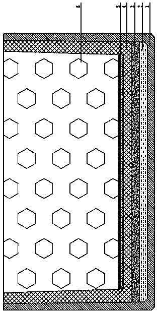
[0027] A method for preparing high-efficiency polycrystalline silicon ingots, the method steps are as follows: mix silica sol and high-purity quartz sand slurry uniformly at a mass ratio of 5:5 to form a mixed slurry, and brush the mixed slurry on the crucible of a polycrystalline silicon ingot casting furnace form a bonding layer at the inner bottom of the bonding layer; then spray 30-mesh high-purity quartz sand on the bonding layer to form a nucleation source layer, the thickness of the nucleation source layer is 1 mm, and then dry at 500 ° C for 2 hours, and then Brush the silicon nitride coating on the upper layer of the nucleation source layer and the inner wall of the crucible. The mass ratio of silicon nitride to water in the silicon nitride coating is 1:3; A complete single-crystal 8-inch silicon wafer is laid flat on the silicon oxide coating as a nucleation source protective layer to prevent the nucleation source from being damaged during the loading process. The thi...

Embodiment 2

[0029] A method for preparing high-efficiency polycrystalline silicon ingots, the method steps are as follows: mix silica sol and high-purity quartz sand slurry uniformly at a mass ratio of 6:4 to form a mixed slurry, and brush the mixed slurry on the crucible of a polycrystalline silicon ingot casting furnace Form a bonding layer at the inner bottom of the bonding layer; then spray 50 mesh high-purity silicon nitride on the bonding layer to form a nucleation source layer, the thickness of the nucleation source layer is 2 mm, and then dry at 550 ° C for 2.5 hours , and then brush the silicon nitride coating on the upper layer of the nucleation source layer and the inner wall of the crucible. The mass ratio of silicon nitride to water in the silicon nitride coating is 1:3; and then on the top of the nucleation source layer A complete 12-inch electronic-grade wafer is laid on the silicon nitride coating as a nucleation source protective layer to prevent the nucleation source from...

Embodiment 3

[0031]A method for preparing high-efficiency polysilicon ingots, the method steps are as follows: mix silica sol and high-purity quartz sand slurry uniformly at a mass ratio of 8:5 to form a mixed slurry, and brush the mixed slurry on the crucible of a polysilicon ingot casting furnace Form a bonding layer at the inner bottom of the bonding layer; brush 80-mesh high-purity quartz sand on the bonding layer to form a nucleation source layer, the thickness of the nucleation source layer is 1.5 mm, and then dry at 600 ° C for 3 hours, Then brush the silicon nitride coating on the upper layer of the nucleation source layer and the inner side wall of the crucible, the mass ratio of silicon nitride and water in the silicon nitride coating is 1:3; The silicon nitride coating is covered with a complete polycrystalline 8-inch silicon wafer as a nucleation source protective layer to prevent the nucleation source from being damaged during the loading process. The thickness of the protectiv...


PUM

PropertyMeasurementUnit
Thicknessaaaaaaaaaa

Abstract

The invention discloses a preparation method of high-efficiency polycrystalline silicon ingots. The method comprises the following steps: uniformly mixing a silicon sol with a highly pure quartz sand slurry to obtain a mixed slurry, and brushing the internal bottom of the crucible in a polycrystalline silicon ingot furnace with the mixed slurry to form an adhesive layer; brushing the adhesive layer with a nucleation source to form a nucleation source layer, and brushing the upper layer of the nucleation source layer and the inner sidewall of the crucible with a silicon nitride coating; adding a solid silicon material to the crucible, and melting to form a silicon fluid; and controlling the gradient of the temperature of the inside of the crucible to make a bottom-up vertical temperature gradient in the crucible, and opening a heat insulation cover to reduce the temperature of the bottom of the crucible. Polycrystalline silicon ingots prepared through the method have the advantages of high conversion efficiency, fine grains and uniform distribution, and corresponding minority carriers have the advantages of long life, few impurity points, regular crystal boundary distribution and no obvious dendrite and twin crystals.

Description

technical field [0001] The invention relates to a method for preparing high-efficiency polycrystalline silicon ingots, belonging to the technical field of polycrystalline silicon ingot casting. Background technique [0002] At present, polycrystalline silicon ingots in the prior art are mainly prepared by using a directional solidification system provided by GT Solar in the United States. This method usually includes steps such as heating, melting, crystal growth, annealing and cooling. During the solidification and growth process, the molten silicon liquid obtains sufficient supercooling degree at the bottom of the crucible to solidify and crystallize by controlling the temperature at the upper end and the opening of the side insulation cover. However, in the initial stage of crystal growth, since the bottom of the crucible has an isotropic structure, the initial nucleation cannot be effectively controlled during the crystallization of silicon liquid, and dislocations are e...

Claims


Application Information

Patent Timeline
IPC IPC(8): C30B28/06C30B29/06
Inventor 刘明权王禄宝施文周司荣进
Owner 江苏美科太阳能科技股份有限公司
Why Eureka
Try Eureka