
Method for manufacturing field-effect transistor based on quantum dot film conducting channel

A conductive channel and field effect transistor technology, which is applied in semiconductor/solid-state device manufacturing, circuits, transistors, etc., can solve the problems of limited overall performance of the device, complicated manufacturing process, limited sensitivity, switching frequency and speed, etc., and achieve device performance Flexible and controllable, simple preparation process and novel preparation method

Active Publication Date: 2014-09-17
FUZHOU UNIV
View PDF5 Cites 17 Cited by
  • Summary
  • Abstract
  • Description
  • Claims
  • Application Information

AI Technical Summary

Problems solved by technology

This traditional thin film field effect transistor based on silicon microelectronics technology has problems such as high equipment requirements, complicated manufacturing process, high cost, limited overall performance of the device, limited sensitivity, switching frequency and speed, etc.
Moreover, with the gradual improvement of people's requirements for high-performance thin-film transistors, thin-film field-effect transistors based on microelectronic silicon technology have been difficult to meet the needs of today's information society for thin-film field-effect transistors with high sensitivity, high switching frequency and switching speed.

Method used


Image

  • Method for manufacturing field-effect transistor based on quantum dot film conducting channel
  • Method for manufacturing field-effect transistor based on quantum dot film conducting channel
  • Method for manufacturing field-effect transistor based on quantum dot film conducting channel

Examples


Embodiment 1

[0033] (1) Weigh 10g of tri-n-octylphosphine oxide, 10g of octadecylamine and 0.5g of cadmium stearate, mix them and treat them under vacuum conditions at 100°C for 0.5 hours. Rise to 320°C to form a cadmium precursor solution;

[0034] (2) Weigh 0.625 mg of selenium powder and dissolve it in 5 ml of tributylphosphine under the protection of nitrogen atmosphere to form a selenium precursor solution;

[0035] (3) Rapidly inject the selenium precursor solution into the cadmium precursor solution, then lower the temperature of the mixed solution to 290 ° C, and keep it at this temperature for 10 hours; and use the chlorobenzene / methanol mixed solution to mix and centrifuge several times to Remove excess reactants and impurity ions to obtain CdSe quantum dot chlorobenzene solution, wherein the concentration of CdSe quantum dots is 5 / cm 3 ;

[0036] (4) Under a nitrogen atmosphere, mix 100 mM 16-mercaptohexadecanoic acid chlorobenzene solution with the prepared CdSe quantum dot chl...

Embodiment 2

[0042] (1) Weigh 20g of tri-n-octylphosphine oxide, 20g of octadecylamine and 2.1g of cadmium stearate, mix them and treat them under vacuum conditions at 115°C for 1.8 hours, then, under the protection of nitrogen atmosphere, the temperature Rise to 320°C to form a cadmium precursor solution;

[0043] (2) Weigh 9.75 mg of selenium powder and dissolve it in 10 ml of tributylphosphine under the protection of nitrogen atmosphere to form a selenium precursor solution;

[0044] (3) Rapidly inject the selenium precursor solution into the cadmium precursor solution, then lower the temperature of the mixed solution to 290 ° C, and keep it at this temperature for 15 hours; and use the chlorobenzene / methanol mixed solution to mix and centrifuge several times to Remove excess reactants and impurity ions, thereby obtaining CdSe quantum dot chlorobenzene solution, that is, the third mixed solution, wherein the concentration of CdSe quantum dots is 8 / cm 3 ;

[0045] (4) Under a nitrogen ...

Embodiment 3

[0051] (1) Weigh 30g of tri-n-octylphosphine oxide, 30g of octadecylamine and 3.7g of cadmium stearate, mix them and treat them under vacuum conditions at 130°C for 3 hours, then, under the protection of nitrogen atmosphere, the temperature Rise to 320°C to form a cadmium precursor solution;

[0052] (2) Under the protection of nitrogen atmosphere, 18.75 mg of selenium powder was weighed and dissolved in 15 ml of tributylphosphine to form a selenium precursor solution;

[0053] (3) Rapidly inject the selenium precursor solution into the cadmium precursor solution, then lower the temperature of the mixed solution to 290 ° C, and keep it at this temperature for 20 hours; and use the chlorobenzene / methanol mixed solution to mix and centrifuge for several times. Remove excess reactants and impurity ions to obtain CdSe quantum dot chlorobenzene solution, wherein the concentration of CdSe quantum dots is 10 / cm 3 ;

[0054] (4) Under a nitrogen atmosphere, mix 250 mM chlorobenzene ...


PUM


Abstract

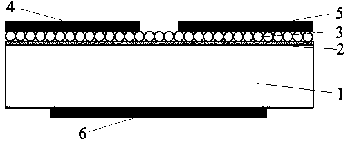
The invention discloses a method for manufacturing a field-effect transistor based on a quantum dot film conducting channel. The advanced quantum dot assembly technology is utilized, a single CdSe quantum dot array film is assembled out on a silicon / silicon dioxide substrate to serve as the conducting channel of the field-effect transistor, Cr / Au composite metal electrodes are formed on the single CdSe quantum dot array film and the substrate silicon of the film through a graphical mask covering evaporation process technology respectively, a source electrode, a drain electrode and a grid electrode are correspondingly led out, the quantum dot channel is effectively packaged and protected by spin-coating of organic matter, and consequently the novel field-effect transistor based on the quantum dot film conducting channel is manufactured out. The manufacturing method is novel, low in manufacturing cost, simple in manufacturing process, accurate and controllable, the manufactured field-effect transistor is provided with the special quantum dot array film conducting channel, the quantum size effect of the quantum dot array film can be fully utilized, and therefore the sensitivity of the transistor is effectively improved, and the method has very significant application value in novel photoelectric devices.

Description

technical field [0001] The invention belongs to the field of semiconductor nanometer materials and devices, and in particular relates to a preparation method of a field effect transistor based on a conductive channel of a quantum dot film layer. Background technique [0002] With the development of science and technology and the progress of society, people are increasingly dependent on information storage, transmission and processing. As the main carrier and material basis of information storage, transmission and processing, semiconductor devices and process technology have become a hot spot for many scientists to study. Field effect transistor, as a very important semiconductor device, plays a vital role in the fields of information storage, transmission and processing. However, up to now, most of the field effect transistors currently used on a large scale are thin film field effect transistors, which are semiconductor devices based on microelectronic silicon technology. ...

Claims


Application Information

Patent Timeline
IPC IPC(8): H01L21/336H01L21/28
CPCB82Y40/00H01L29/1033H01L29/66568
Inventor 杨尊先郭太良胡海龙徐胜吕军
Owner FUZHOU UNIV
Learn More