Eureka AIR delivers breakthrough ideas for toughest innovation challenges, trusted by R&D personnel around the world.

Silicon carbide mesoporous array material and manufacturing method of silicon carbide mesoporous array material

A silicon carbide mesoporous and array technology, which is applied in metal material coating process, gaseous chemical plating, manufacturing of microstructure devices, etc., can solve the problems of uneven longitudinal distribution, thickness of cap layer and transition layer, etc., and achieves convenient preparation. , Simplified preparation equipment, strong reproducible effect

Inactive Publication Date: 2014-10-29
SHANGHAI NORMAL UNIVERSITY
View PDF7 Cites 7 Cited by
  • Summary
  • Abstract
  • Description
  • Claims
  • Application Information

AI Technical Summary

Problems solved by technology

[0003] The purpose of the present invention is to overcome the present situation of sample cap layer and transition layer thickness and uneven longitudinal distribution in the prior art, and propose a silicon carbide mesoporous array material and its preparation method

Method used


Image

  • Silicon carbide mesoporous array material and manufacturing method of silicon carbide mesoporous array material

Examples


Embodiment Construction

[0019] Below in conjunction with accompanying drawing and embodiment the present invention is described in further detail

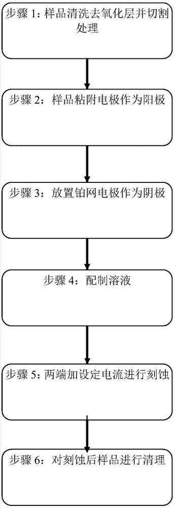
[0020] A preparation process of a mesoporous array based on a heavily doped n-type 4H-SiC substrate described in an embodiment of the present invention (such as figure 1 shown), including the following steps:

[0021] Step 1, prepare heavily doped n-type 4H-SiC pre-etched samples.

[0022] The sample is a wafer with a size of 100cm 2 , cut at 4°, polished on both sides, obtained after cleaning by strict semiconductor process and cut into 1.2cm×1.2cm square pieces by pre-etching samples, and then passed through hydrofluoric acid with a volume ratio of 1:1 ( 49%) and ethanol (99%) solution to remove the surface oxide layer.

[0023] Step 2, cut the dual-lead copper foil to an area of ​​1cm 2 square, and then uniformly adhered to the Si surface of the sample.

[0024] Step 3, fix the sample at the anode position of the etching tank, and place the platin...


PUM

PropertyMeasurementUnit
thicknessaaaaaaaaaa
pore sizeaaaaaaaaaa
thicknessaaaaaaaaaa

Abstract

The invention discloses a silicon carbide mesoporous array material and a manufacturing method of the silicon carbide mesoporous array material, particularly discloses the manufacturing technology of a high-temperature-resistant and corrosion-resistant large-energy-gap silicon carbide material with even mesoporous arrays, and relates to the technical field of porous semiconductor device manufacturing. The silicon carbide mesoporous array material is characterized in that dual-conduction copper foil is pasted to the Si face of a sample to simplify preparation work of back electrode metal contact manufacturing needed by anodizing. Compared with double-groove electrochemical corrosion, parts of electrolytes are saved, and manufacturing instruments are simplified. In the manufacturing process, the appropriate pulse frequency and the appropriate standing time are selected for applying constant pulse currents to two electrodes, and the mesoporous arrays which are coincident in longitudinal hole diameter are obtained, wherein cap transition layers are only 1 omicron m, and the thicknesses of porous layers are 25 omicron m. Compared with an existing manufacturing process, the manufacturing method has the advantages of being high in repeatability, high in rate of finished products and the like. A solid technological and material base is provided for applying third-generation semiconductor silicon carbide products which are high in carrier mobility, high in heat conductivity, resistant to corrosion, resistant to high pressure and the like in the fields of power electronics and space flight and aviation.

Description

technical field [0001] The invention relates to the technical field of preparation of porous semiconductor devices, and specifically refers to a preparation technology of a wide bandgap silicon carbide material with high temperature resistance, corrosion resistance and uniform mesoporous array. Background technique [0002] As the third-generation semiconductor, silicon carbide has been used in the fields of power electronics and aerospace, and it has high carrier mobility, thermal conductivity, corrosion resistance, and high-voltage resistance of silicon carbide, which are superior to the first generation. The advantages of semiconductors make it expected to replace the application status of first-generation semiconductors in various fields. In the field of semiconductors, microstructure modulation of semiconductor materials (MEMS) has received extensive attention. Silicon, as the first generation of semiconductors, has relatively mature technology in this area. It is worth...

Claims


Application Information

Patent Timeline
Patent Type & Authority Applications(China)
IPC IPC(8): B81B7/04B81C1/00
Inventor 谈嘉慧何鸿张永平陈之战石旺舟
Owner SHANGHAI NORMAL UNIVERSITY
Why Eureka
Eureka Blog
Learn More