Method for manufacturing photoelectric detector based on integrated chip with alloy semiconductor nano-structure

A photodetector and nanostructure technology, applied in the field of photodetection, can solve the problems of uneven response and high cost of photodetectors, and achieve the effects of high-sensitivity photoconductive detection, low production cost, and reduced production cost

Inactive Publication Date: 2014-11-12
BEIJING INSTITUTE OF TECHNOLOGYGY
View PDF3 Cites 4 Cited by
  • Summary
  • Abstract
  • Description
  • Claims
  • Application Information

AI Technical Summary

Problems solved by technology

[0007] The purpose of the present invention is to solve the problem of inhomogeneous response in the detection range and high cost of making large-area photodetectors in the existing photoelectric detection technology, and to provide a kind of photodetector based on alloy

Method used


Image

  • Method for manufacturing photoelectric detector based on integrated chip with alloy semiconductor nano-structure
  • Method for manufacturing photoelectric detector based on integrated chip with alloy semiconductor nano-structure
  • Method for manufacturing photoelectric detector based on integrated chip with alloy semiconductor nano-structure

Examples


Embodiment 1

[0032] The fabrication of a photodetector based on an alloy semiconductor nanostructure integrated substrate, the specific steps are as follows:

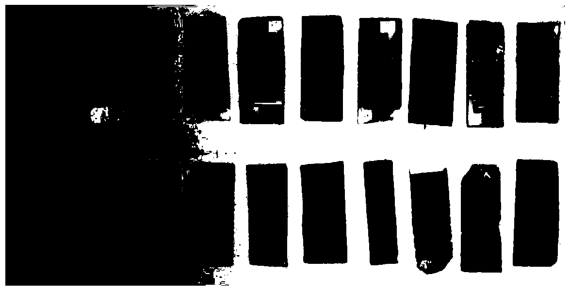
[0033] 1. Stir cadmium sulfide and cadmium selenide evenly in a mortar for 10 minutes according to the molar ratio of 1:1; clean the silicon wafer with absolute ethanol in an ultrasonic cleaner for 10 minutes, and after drying, use an ion sputtering instrument to plate gold for 60 seconds , Clean small porcelain containers and high temperature resistant glass containers for later use. Then put the mixture of CdS (cadmium sulfide) and CdSe (cadmium selenide) into the porcelain container, and place the porcelain container in the center of the high temperature resistant glass container. Put a gold-plated silicon wafer in another porcelain container, place it downstream of the airflow of the high-temperature-resistant glass container, 11 cm away from the center of the high-temperature-resistant glass container. Put the high-temperature...

Embodiment 2

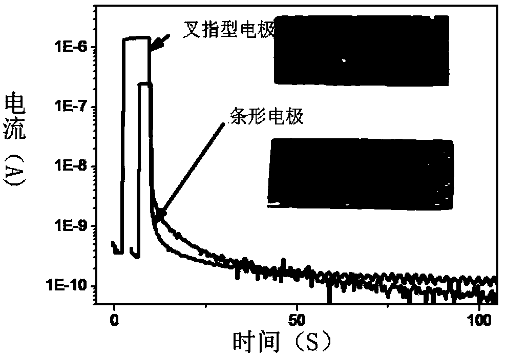
[0039] Based on the semiconductor test system (Keithley-4200), the photoconductive properties of CdSSe alloy nanostructure substrates plated with different electrode materials, different electrode thicknesses, and different electrode shapes with gradient components under the irradiation of polychromatic light (white light), and The change of photocurrent. The steps are:

[0040]1. Stir cadmium sulfide and cadmium selenide uniformly in a mortar for 15 minutes according to the molar ratio of 1:1; silicon wafer (n-type silicon, crystal orientation ) is cleaned in an ultrasonic cleaner with absolute ethanol for 10 minutes. Minutes, after drying, gold-plate with ion sputtering device for 60 seconds, and clean small porcelain containers and high-temperature-resistant glass containers for later use. Then put the mixture of CdS (cadmium sulfide) and CdSe (cadmium selenide) into the porcelain container, and place the porcelain container in the center of the high temperature resistant ...

Embodiment 3

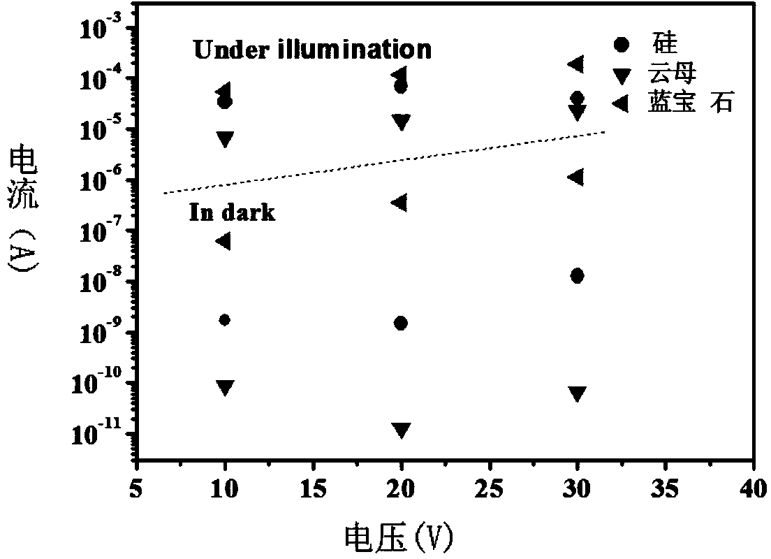
[0047] Based on the semiconductor test system, the alloy nanostructures grown under different substrates were tested, focusing on the photoconductive properties of the nanostructures synthesized on various substrates, and the change of photocurrent / dark current. The steps are:

[0048] 1. Stir cadmium sulfide and cadmium selenide uniformly in a mortar for 20 minutes according to the molar ratio of 1:1; different thicknesses and different types of single substrate [silicon wafer (n-type silicon, crystal orientation ), Gem slices, mica slices] were cleaned in an ultrasonic cleaner with absolute ethanol for 10 minutes, and after drying, they were gold-plated with an ion sputtering instrument for 60 seconds, and the small porcelain containers and high-temperature-resistant glass containers were cleaned for later use. Then put the mixture of CdS (cadmium sulfide) and CdSe (cadmium selenide) into the porcelain container, and place the porcelain container in the center of the high te...


PUM

PropertyMeasurementUnit
Thicknessaaaaaaaaaa
Widthaaaaaaaaaa

Abstract

The invention relates to a method for manufacturing a photoelectric detector based on an integrated chip with an alloy semiconductor nano-structure and belongs to the field of photoelectric detection. According to the method for manufacturing the photoelectric detector which is high in broadband sensitivity, large in scale and low in cost based on the integrated chip which is integrally grown on a single substrate and provided with the one-dimensional CdSSe ternary alloy semiconductor nano-structure with the gradually-changing band gap, electrode structures in different shapes and with different widths are manufactured on the chip on which the CdSxSe1-X ( x ranging from zero to one) nano-structure which comprises different components and provided with the gradually-changing band gap is grown in a gradually-changing mode through heat evaporation or electron beam evaporation, and finally, the photoconductive detector which is high in broadband sensitivity and can cover the whole visible region and the near ultraviolet region is manufactured by taking the whole chip as a detecting unit and electrically connecting the whole chip with a nonlinear current amplifying circuit.

Description

technical field [0001] The invention relates to the manufacture of a photodetector based on an alloy semiconductor nanostructure integrated substrate, belonging to the field of photoelectric detection. Background technique [0002] Semiconductor photoconductive detectors are widely used in various fields of national economy and military, such as in the visible light or near-infrared band, mainly used for radiation measurement and detection, photometry, camera tube target surface, etc.; in the infrared band, mainly used for Missile guidance, infrared thermal imaging, etc. Among them, high-sensitivity miniature photodetectors with broadband spectral response have gradually become one of the research targets in the field of photodetection due to their great application potential in the fields of optical sensing and precise spectral measurement. [0003] There are many deficiencies in the photodetectors currently on the market. For example, silicon (indirect bandgap semiconduct...

Claims


Application Information

Patent Timeline
IPC IPC(8): H01L31/18
CPCH01L31/02966H01L31/0352H01L31/09H01L31/1832Y02P70/50
Inventor 刘瑞斌
Owner BEIJING INSTITUTE OF TECHNOLOGYGY
Why Eureka
Try Eureka