A Novel Photoconductive Detector

A detector and photoconductive technology, used in semiconductor devices, circuits, electrical components, etc., can solve the problems of low product yield, difficult preparation, and difficulty in mass production, and achieve the reduction of resistance value, lower resistivity, The effect of increasing the carrier concentration

Inactive Publication Date: 2017-07-07
UNIV OF ELECTRONICS SCI & TECH OF CHINA
View PDF3 Cites 0 Cited by
  • Summary
  • Abstract
  • Description
  • Claims
  • Application Information

AI Technical Summary

Problems solved by technology

[0005] The technical problem to be solved by the present invention is to overcome the difficulty of preparation, low product yield, high process cost, difficulty in mass production and low device aperture ratio of traditional photoconductive detectors due to the use of interdigitated electrode structures. Shortcomi

Method used


Image

  • A Novel Photoconductive Detector
  • A Novel Photoconductive Detector
  • A Novel Photoconductive Detector

Examples


Embodiment

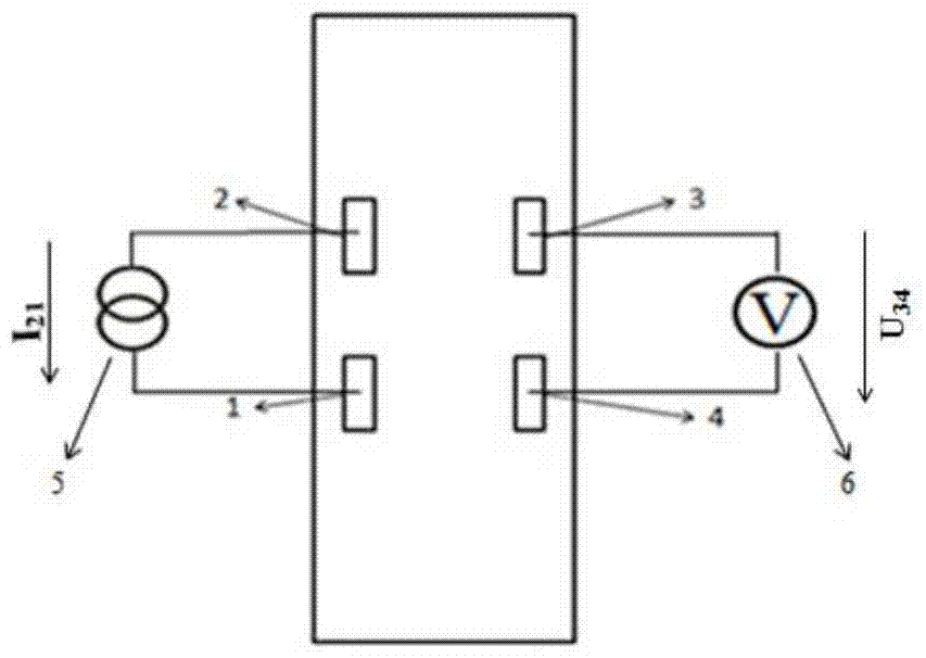
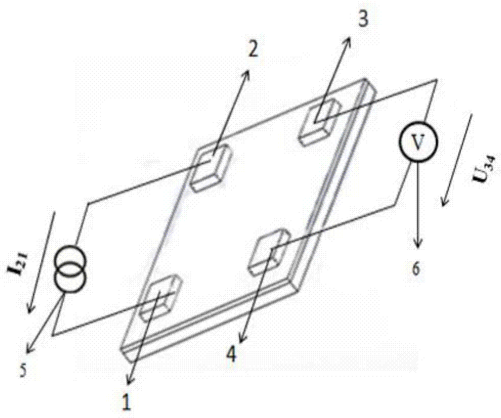
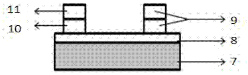
[0024] A new type of photoconductive detector, such as image 3 As shown, from bottom to top: sapphire substrate 7 (c-plane Al 2 o 3 ), deposited on a sapphire substrate with a thickness of about 100nm β-Ga 2 o 3 Thin film 8, located in β-Ga 2 o 3 A patterned electrode layer 9 on the film; wherein, the patterned electrode layer includes a first electrode 1, a second electrode 2, a third electrode 3, and a fourth electrode 4, and the first electrode, the second electrode, and the third electrode The relative position of the fourth electrode pattern is an arbitrary quadrangle, and the first electrode, the second electrode, the third electrode, and the fourth electrode are arranged clockwise or counterclockwise, such as figure 1 shown; the first electrode is grounded, a constant current is connected between the first electrode and the second electrode, and the first electrode, the second electrode, the third electrode, and the fourth electrode are deposited on β-Ga 2 o 3 A...


PUM


Abstract

A novel photoconductive detector belongs to the field of electronic information materials and components. The photoconductive detector consists of an active layer and a patterned electrode layer from bottom to top, wherein the patterned electrode layer includes a first electrode, a second electrode, a third electrode, and a fourth electrode. The relative position of the second electrode, the third electrode and the fourth electrode pattern is an arbitrary quadrilateral structure. The first electrode, the second electrode, the third electrode and the fourth electrode are arranged clockwise or counterclockwise. When working, the A constant current power supply is connected between the first electrode and the second electrode, and a voltage value is tested by a voltage measuring device between the third electrode and the fourth electrode, and the optical signal is identified through the change of the voltage value. The photoconductive detector of the present invention has lower requirements on the size of the electrode structure, and its preparation does not require photolithography technology, and the preparation process is simpler, which helps to improve the yield of products and reduce production costs, and the aperture ratio of the device is greatly improved.

Description

technical field [0001] The invention belongs to the field of electronic information materials and components, and in particular relates to a novel photoconductive detector, which can be used for ultraviolet or infrared detection. Background technique [0002] In recent years, photoelectric detection technology has developed rapidly and is widely used, mainly including infrared detection technology, ultraviolet detection technology, laser detection technology and photoelectric comprehensive detection technology. Among them, using infrared detection technology, infrared night vision devices and thermal imagers can be prepared for long-distance investigation, surveillance, tracking and detection of camouflage, etc.; ultraviolet detection technology can be used for combustion process detection, ultraviolet leakage inspection, fire prevention and missile detection. Laser detection technology is generally used in laser range finders, laser radars, laser target indicators, etc.; ph...

Claims


Application Information

Patent Timeline
IPC IPC(8): H01L31/09H01L31/0224
CPCH01L31/022408H01L31/09
Inventor 钱凌轩夏勇刘兴钊张万里李言荣
Owner UNIV OF ELECTRONICS SCI & TECH OF CHINA
Why Eureka
Try Eureka