Preparation method for large-area lead iodide thick film and implementation equipment thereof

A lead iodide, large-area technology, applied in the field of preparation of large-area lead iodide polycrystalline thick films, can solve the problems of small size, poor uniformity of polycrystalline thick films, and corrosion of crystalline substrates, to overcome crystal orientation The change of the crystallization preferred orientation, the effect of increasing the grain size and junction

Inactive Publication Date: 2014-11-26
朱 兴华 +1
View PDF4 Cites 11 Cited by
  • Summary
  • Abstract
  • Description
  • Claims
  • Application Information

AI Technical Summary

Problems solved by technology

The thermal evaporation method can prepare polycrystalline thick films with excellent performance, but the existing technology uses small-area point-like evaporation sources to prepare lead iodide thick films, which leads to poor uniformity of the prepared large-area polycrystalline thick films. As the temperature of the substrate changes, the crystallographic orientation and grain size of the thick film will change significantly, resulting in a greatly reduced density and conversion performance of the polycrystalline film (M. Schieber, N. Zamoshchik, O. Khakhan, Journal of Crystal Growth 310 (2008) 3168–3173)
The lead iodide polycrystalline film prepared by the solution method is difficult to obtain a large-area thick film with a thickness of more than 100 microns, and it is easy to introduce various impurities. Various defects caused by impurities seriously reduce the detection performance of the material. The polycrystalline film must be annealed, and different annealing processes have a great influence on the performance of the polycrystalline film. Crystallization in the solution to prepare the polycrystalline film, the solution will cause different degrees of corrosion on the crystallization substrate, thus affecting Device performance (J.P. Ponpon, M. Amann, Thin Solid Films 394 (2001), 277-283)
The lead iodide thick film is prepared by the coating process by the screen printing method, which can realize the preparation of a hundred micron thick film. On the bottom, the lead iodide thick film is prepared by low temperature heat treatment. The grain structure of the prepared lead iodide thick film is incomplete, the size is small, the grain orientation is poor, and the grain gap is large, and the gap is filled with residual organic matter. , greatly reducing the transport efficiency of carriers (such as the literature Min-seok Yun, Sung-ho Cho, Rena Lee, Japanese Journal of Applied Physics 49 (2010) 041801)
None of the above methods and technologies is an ideal method for preparing a large-area lead iodide thick film with stable structure and excellent performance. Industrial production urgently needs to develop new methods for preparing large-area lead iodide thick film materials to meet the needs of manufacturing large-area high-energy ray flat plates. The need for detector direct conversion layers

Method used


Image

  • Preparation method for large-area lead iodide thick film and implementation equipment thereof
  • Preparation method for large-area lead iodide thick film and implementation equipment thereof

Examples


Embodiment 1

[0032] In this embodiment, the preparation area is 5×5cm 2 , lead iodide polycrystalline thick film with a thickness of 700 microns.

[0033] The processing steps of this example are as follows:

[0034] 1. Put the substrate 2 in ethanol for 30 minutes for ultrasonic cleaning, then put it in acetone for 30 minutes, and then put it in a vacuum oven for drying;

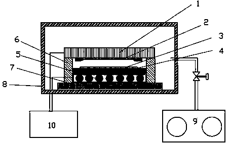
[0035] 2. Install the cleaned substrate on the directional graphite heat dissipation plate 1 to ensure that the upper surface of the substrate is closely attached to the lower surface of the graphite heat dissipation plate to facilitate heat dissipation and substrate temperature uniformity;

[0036] 3. Spread the raw material high-purity lead iodide powder (99.99%) 3 on the raw material carrier graphite plate 4 located on the flat heater 5, the area of ​​the raw material is about 6×6cm 2 , the thickness is between 0.5-1.3 mm; then place the temperature sensor on the edge of the raw material to contact with both the ra...

Embodiment 2

[0040] In this embodiment, the preparation area is 50×50cm 2 , lead iodide polycrystalline thick film with a thickness of 500 microns.

[0041] The technology of the present embodiment is basically the same as the technology of embodiment 1, the difference is that the area of ​​the raw material tiled on the raw material carrier graphite sheet 4 is about 52 × 52 cm 2 , the thickness is between 0.5-1.0 mm, the distance between the lower surface of the substrate and the upper surface of the raw material is 50 mm, and the vacuum degree of the vacuum chamber 8 is 5.0×10 -2 Pa, the heating rate of the plate heater is 5°C / min, the raw material is heated to 300°C, and kept for 60 minutes.

Embodiment 3

[0043] In this embodiment, the preparation area is 20×20cm 2 , lead iodide polycrystalline thick film with a thickness of 1000 microns.

[0044] The technology of the present embodiment is basically the same as the technology of embodiment 1, the difference is that the area of ​​the raw material tiled on the raw material carrier graphite sheet 4 is about 22 × 22 cm 2 , the thickness is between 1.1-2.0 mm, the distance between the lower surface of the substrate and the upper surface of the raw material is 30 mm, and the vacuum degree of the vacuum chamber 8 is 1.0×10 -5 Pa, the heating rate of the plate heater is 3°C / min, the raw material is heated to 220°C, and kept for 40 minutes.


PUM

PropertyMeasurementUnit
thicknessaaaaaaaaaa
thicknessaaaaaaaaaa
thicknessaaaaaaaaaa

Abstract

The invention discloses a preparation method for a large-area lead iodide thick film and implementation equipment thereof. According to the invention, in a vacuum cavity of the equipment, the raw material high purity lead iodide powder is spread on a raw material carrier graphite sheet, which is placed on a flat heater, a directional heat dissipation plate equipped with a substrate at the bottom is supported by a quartz block over the raw material, in an environment with a vacuum degree of 10<-1>Pa-10<-5>Pa, starting the flat heater to heat the raw material to gasify it, and the raw material gas condenses and deposits at the low temperature substrate, thus forming the dense lead iodide polycrystal film. With the method and equipment provided by the invention, the lead iodide polycrystal thick film with a thickness of 50-1000 micrometers, an area of 5*5cm<2>-50*50cm<2>, uniform thickness and excellent properties can be prepared on the substrate. Also, the preparation process is simple and low in cost, thus being suitable for industrial mass production.

Description

technical field [0001] The invention relates to the preparation technology of a large-area compound semiconductor polycrystalline film, in particular to a preparation method and equipment for preparing a large-area lead iodide polycrystalline thick film. Background technique [0002] Lead iodide (PbI 2 ) as a direct conversion material for room temperature ionizing radiation detection and digital flat panel X-ray imaging has very important application prospects. The atomic number of lead iodide material is large (Z Pb =82,Z I =53), it has high stopping power and large absorption for high-energy rays (such as X-rays, γ-rays), and a large band gap (E g =2.3-2.5eV), the intrinsic resistivity is high, the device made of it has low leakage current, low noise, and can work normally in the temperature range from room temperature to 110 °C. Since it is necessary to reduce the radiation energy and dose as much as possible in human medical radiography to reduce the damage to the hu...

Claims


Application Information

Patent Timeline
Patent Type & Authority Applications(China)
IPC IPC(8): C23C14/24C23C14/06
Inventor 朱兴华孙辉
Owner 朱 兴华
Why Eureka
Try Eureka