Graphical method for graphene thin film, functional device and application of graphene thin film
A technology of graphene film and functional devices, which is applied in the manufacture of semiconductor/solid-state devices, instruments, electrical components, etc. It can solve the problems of non-positioning voids, inability to realize arbitrary cutting of graphene, and deterioration of film performance, so as to prevent non-positioning Defects, avoiding the problem of rough edges of graphics, and the effect of convenient application
- Summary
- Abstract
- Description
- Claims
- Application Information
AI Technical Summary
Problems solved by technology
Method used
Image
Examples
Embodiment 1
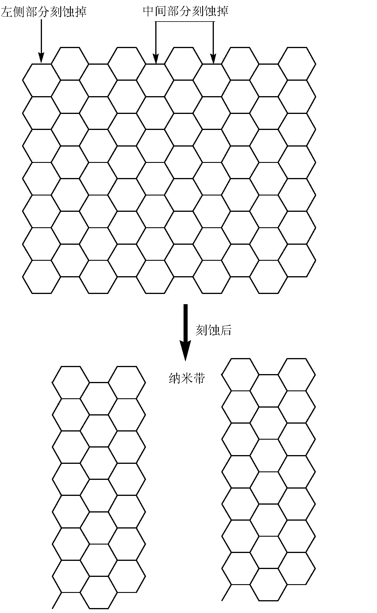
[0026] This embodiment is used for the patterning of graphene film to obtain nanoribbons, proceed as follows:
[0027] a. Spray a layer of epoxy resin with a thickness of 10 μm on the surface of the single-layer graphene sample prepared on the copper foil by electrostatic spraying, and remove the solvent in a low-temperature oven at 30°C to obtain Cu / GN / ring Oxygen resin sample A1;
[0028] b. The sample A1 is exposed on an exposure machine using two nanobelts with a width of 100 μm in the light-transmitting area of the film, and the exposed sample B1 is obtained;
[0029] c. Soak sample B1 in a sodium carbonate solution with a temperature of 25°C and a concentration of 1% for 30 minutes, remove the epoxy resin in the unexposed area, and then clean it with deionized water to obtain sample C1;
[0030] d. Place sample C1 in an oxygen plasma atmosphere, control the temperature at 60°C, and etch for 3 minutes to etch away the graphene in the area not protected by epoxy resin t...
Embodiment 2
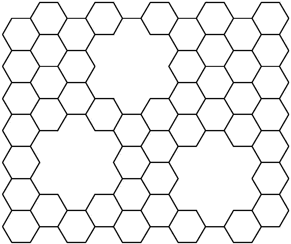
[0033] This embodiment is used for the patterning of graphene thin film to obtain flower pattern, proceed as follows:
[0034] a. Spray-print a layer of epoxy resin with a thickness of 8 μm on the surface of the single-layer graphene sample that has been prepared on the copper foil, and remove the solvent in a low-temperature oven at 30°C to obtain Cu / GN / epoxy resin sample A2;
[0035] b. Use the masked area of sample A2 as figure 2 Cover the negative film in the blank area shown, and then place it on the exposure machine for exposure to obtain the exposed sample B2;
[0036] c. Soak sample B2 in a sodium carbonate solution with a temperature of 28°C and a concentration of 1.2% for 30 minutes, remove the epoxy resin in the unexposed area, and then clean it with deionized water to obtain sample C2;
[0037] d. Place sample C2 in an oxygen plasma atmosphere, control the temperature at 70°C, and etch for 8 minutes to etch away the graphene in the area not protected by epox...
Embodiment 3
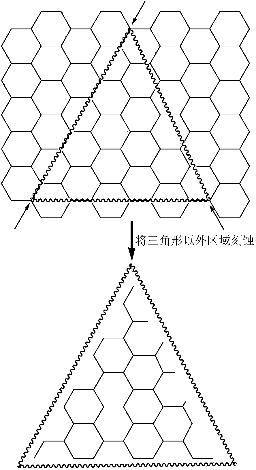
[0040] The present embodiment is used for the patterning of graphene thin film and obtains triangular pattern and carries out as follows:
[0041] a. Print a layer of epoxy resin with a thickness of 5 μm on the surface of the single-layer graphene sample prepared on the copper foil by screen printing, and remove the solvent in a low-temperature oven at 30°C to obtain Cu / GN / epoxy resin sample A3;
[0042] b. Expose sample A3 using a triangle with a side length of 200 μm in the light-transmitting area of the film, and place it on an exposure machine for exposure to obtain exposed sample B3;
[0043] c. Soak sample B3 in a sodium carbonate solution with a temperature of 30°C and a concentration of 0.8% for 25 minutes, remove the epoxy resin in the unexposed area, and then clean it with deionized water to obtain sample C3;
[0044] d. Place sample C3 in an oxygen plasma atmosphere, control the temperature at 55°C, and etch for 6 minutes to etch away the graphene in the area n...
PUM
| Property | Measurement | Unit |
|---|---|---|
| Thickness | aaaaa | aaaaa |
| Width | aaaaa | aaaaa |
Abstract
Description
Claims
Application Information
 - R&D Engineer
- R&D Manager
- IP Professional
- Industry Leading Data Capabilities
- Powerful AI technology
- Patent DNA Extraction
Browse by: Latest US Patents, China's latest patents, Technical Efficacy Thesaurus, Application Domain, Technology Topic, Popular Technical Reports.
© 2024 PatSnap. All rights reserved.Legal|Privacy policy|Modern Slavery Act Transparency Statement|Sitemap|About US| Contact US: help@patsnap.com


